|
Product Details:
|
| Density(g/cm3): | 3.515 | Young’s Modulus(PGa): | 1050 |
|---|---|---|---|
| Product Name: | CVD Diamond Substrates | Fracture Toughness(MPa·m1/2): | 1~8 |
| Firction Coefficient: | 0.1 | Thermal Conductivity(300K,Wm·K): | 1000~2000 |
| Highlight: | 100ppb single crystal wafer,0.3mm crystal quartz wafer,Heat Sink single crystal wafer |
||
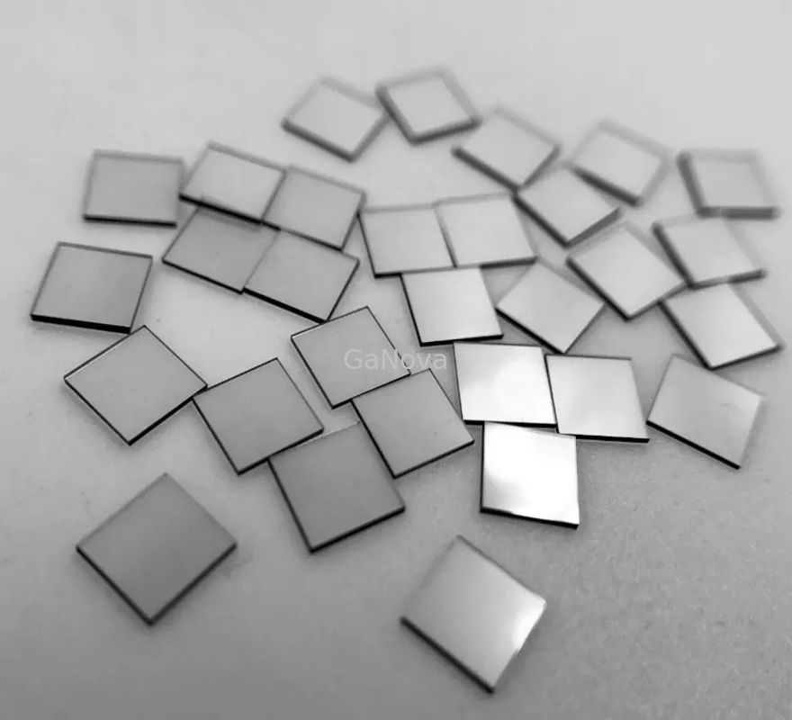
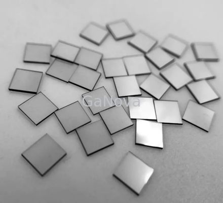
3*3mm²*0.3mm Electronic Grade Single Crystal Diamond,N Content<100ppb, XRD<0.015º For Heat Sink
Overview
Remarkable progress in CVD methods of diamond synthesis has made it possible to prepare diamonds suitable for radiation detection with tailored properties on routine basis. Continuing improvements in CVD methods offer exciting future advancements and large area homo-epitaxial grown single crystal diamond plates/films. There are many applications such as RF diodes, BJT, FET, MEMS and electronic industry due to promising results shown by CVD diamonds. Continued innovation and sustained efforts wold give direction in medical field such as radiotherapy dosimeter.
Specification
| properties | Synthetic diamond | |
| Density(g/cm3) | 3.515 | Intrinsic properties |
| Young’s modulus(PGa) | 1050 |
Mechanical property |
| Hardness(PGa) |
70~120single crystal 60~100 polycrystalline |
|
| Breaking strength |
2.5-3GPasingle crystal 200-1100MPa polycrystalline |
|
| Fracture toughness(MPa·m1/2) | 1~8 | |
| Firction coefficient | 0.1 | |
| Thermal conductivity(300K,Wm·K) | 1000~2000 | Thermal properties |
| Coefficient of thermal expansion(×10-6/℃) | 1(room temperature) | |
| Rerfractive index(590nm) | 2.4 | Optical properties |
| Light transmittance | 225nm to far infrared | |
| Band gap width(ev) | 5.47 | Electrical properties |
| Resistivity(Ω·cm) | >1010 | |
| Electron mobility(cm2/V·s) | 4500 | |
| Hole mobility(cm2/V·s) | 3800 | |
| Dielectric constant | 5.5 | Dielectric properties |
| Dielectric losses | <2×10⁻⁴ |
About Us
We specialize in processing a variety of materials into wafers, substrates and customized optical glass parts.components widely used in electronics, optics, opto electronics and many other fields. We also have been working closely with many domestic and oversea universities, research institutions and companies, provide customized products and services for their R&D projects. It's our vision to maintaining a good relationship of cooperation with our all customers by our good reputations.
FAQ
Q: Are you trading company or manufacturer ?
We are factory.
Q: How long is your delivery time?
Generally it is 3-5 days if the goods are in stock.
or it is 7-10 days if the goods are not in stock, it is according to quantity.
Q: Do you provide samples ? is it free or extra ?
Yes, we could offer the sample for free charge but do not pay the cost of freight.
Q: What is your terms of payment ?
Payment <=5000USD, 100% in advance.
Paymen >=5000USD, 80% T/T in advance , balance before shippment.
Contact Person: Xiwen Bai (Ciel)
Tel: +8613372109561