|
Product Details:
|
| Surface Orientation: | A-Plane(11-20) | Material: | High Purity Al₂O₃(>99.995%) |
|---|---|---|---|
| Thickness: | 430 ±15μm | R-plane: | R9 |
| Diameter: | 50.8 ±0.10 | Wafer Edge: | R-type |
| Highlight: | Sapphire Wafer EPI Ready,led sapphire substrate R9,sapphire wafer A Plane |
||
High purity Al2O3>99.995% Sapphire Substrate Wafer Mirror Polished EPI-Ready
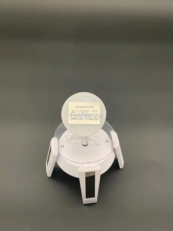
JDCD08-001-001 Diameter 50mm Sapphire substrate wafer , Thk 430μm, crystal orientation C/M0.2, OF length (mm) 16 LED chip,substrate material
Sapphire Substrate Sapphire Substrate makes for superior window material for many IR applications from 3µm to 5µm, for they offer resistant to high temperature, thermal shock, water and sand erosion, small dielectric loss, excellent electrical insulation, with important mechanical and chemical characteristics, and scratching. We have C-Plane R-Plane Sapphire Substrates. C-plane sapphire substrates used for developing III-V and II-VI compounds like GaN for blue LED and laser diodes.
|
Parameters |
Specification | ||
| Unit | Target | Tolerance | |
| Material | High purity Al2O3(>99.995%) | ||
| Diameter | mm | 50.8 | ±0.10 |
| Thickness | μm | 430 | ±15 |
| Surface Orientation | C-Plane(0001) | ||
| -Off Angle toward M-axis | degree | 0.20 | ±0.10 |
| -Off Angle toward A-axis | degree | .00 | ±0.10 |
| Flat Orientation | A-Plane(11-20) | ||
| -Flat Off-set Angle | degree | 0.0 | ±0.2 |
| Flat Lenght | mm | 16.0 | ±1 |
| R-plane | R9 | ||
| Front surface Roughness(Ra) | nm | <0.3 | |
| Back surface Roughness | μm | 0.8~1.2μm | |
| Front surface Quality | Mirror Polished,EPI-Ready | ||
| Wafer edge | R-type | ||
| Chamfer amplitude | μm | 80-160 | |
| Included angle radian between flat edge and round edge | mm | R=9 | |
| TTV | μm | ≤5 | |
| LTV(5x5mm) | μm | ≤1.5 | |
| Bow | μm | 0~-5 | |
| Warp | μm | ≤10 | |
| Laser mark | As customer required | ||
About Us
We specialize in processing a variety of materials into wafers, substrates and customized optical glass parts.components widely used in electronics, optics, opto electronics and many other fields. We also have been working closely with many domestic and oversea universities, research institutions and companies, provide customized products and services for their R&D projects. It's our vision to maintaining a good relationship of cooperation with our all customers by our good reputations.
FAQ
Q: Are you trading company or manufacturer ?
We are factory.
Q: How long is your delivery time?
Generally it is 3-5 days if the goods are in stock.
or it is 7-10 days if the goods are not in stock, it is according to quantity.
Q: Do you provide samples ? is it free or extra ?
Yes, we could offer the sample for free charge but do not pay the cost of freight.
Q: What is your terms of payment ?
Payment <=5000USD, 100% in advance.
Paymen >=5000USD, 80% T/T in advance , balance before shippment.
Contact Person: Xiwen Bai (Ciel)
Tel: +8613372109561