|
Product Details:
|
| Density(g/cm3): | 3.515 | Young’s Modulus(PGa): | 1050 |
|---|---|---|---|
| Product Name: | CVD Diamond Substrates | Fracture Toughness(MPa·m1/2): | 1~8 |
| Thermal Conductivity(300K,Wm·K): | 1000~2000 | Light Transmittance: | 225nm To Far Infrared |
| Highlight: | 0.3mm Single Crystal Diamond,chemical vapor deposition substrates,Single Crystal Diamond 225nm |
||
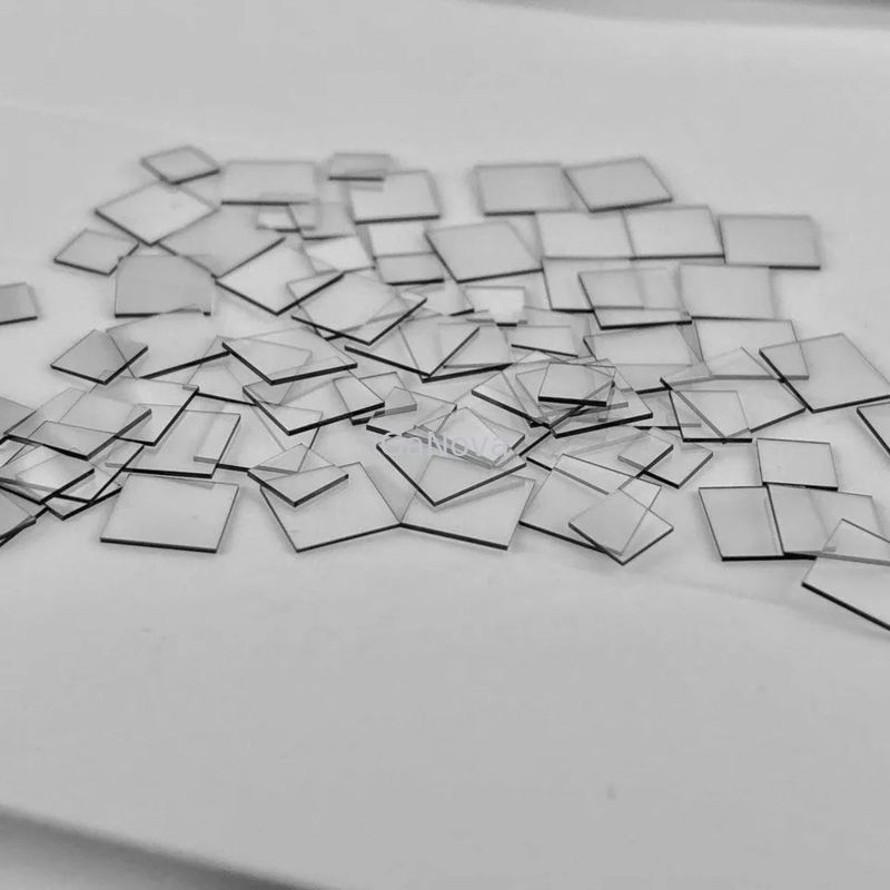
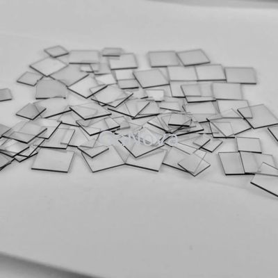
3*3mm²*0.3mm Electronic Grade Single Crystal Diamond 225nm To Far Infrared
3*3mm²*0.3mm Electronic Grade Single Crystal Diamond,N Content<100ppb, XRD<0.015º For Heat Sink
Overview
Due to its unique combination of superior material properties, diamond is often referred to as the ultimate semiconductor material for high-power electronics. Lack of wafer-size electronic-grade single crystals was always considered a crucial bottleneck for the device development and the subsequent transfer to industrial processes. Over the last years, significant progress has been made for the classical high-pressure high-temperature (HPHT) method and in particular for the alternative chemical vapor deposition (CVD) technique.
Specification
| properties | Synthetic diamond | |
| Density(g/cm3) | 3.515 | Intrinsic properties |
| Young’s modulus(PGa) | 1050 |
Mechanical property |
| Hardness(PGa) |
70~120single crystal 60~100 polycrystalline |
|
| Breaking strength |
2.5-3GPasingle crystal 200-1100MPa polycrystalline |
|
| Fracture toughness(MPa·m1/2) | 1~8 | |
| Firction coefficient | 0.1 | |
| Thermal conductivity(300K,Wm·K) | 1000~2000 | Thermal properties |
| Coefficient of thermal expansion(×10-6/℃) | 1(room temperature) | |
| Rerfractive index(590nm) | 2.4 | Optical properties |
| Light transmittance | 225nm to far infrared | |
| Band gap width(ev) | 5.47 | Electrical properties |
| Resistivity(Ω·cm) | >1010 | |
| Electron mobility(cm2/V·s) | 4500 | |
| Hole mobility(cm2/V·s) | 3800 | |
| Dielectric constant | 5.5 | Dielectric properties |
| Dielectric losses | <2×10⁻⁴ |
About Us
We specialize in processing a variety of materials into wafers, substrates and customized optical glass parts.components widely used in electronics, optics, opto electronics and many other fields. We also have been working closely with many domestic and oversea universities, research institutions and companies, provide customized products and services for their R&D projects. It's our vision to maintaining a good relationship of cooperation with our all customers by our good reputations.
FAQ
Q: Are you trading company or manufacturer ?
We are factory.
Q: How long is your delivery time?
Generally it is 3-5 days if the goods are in stock.
or it is 7-10 days if the goods are not in stock, it is according to quantity.
Q: Do you provide samples ? is it free or extra ?
Yes, we could offer the sample for free charge but do not pay the cost of freight.
Q: What is your terms of payment ?
Payment <=5000USD, 100% in advance.
Paymen >=5000USD, 80% T/T in advance , balance before shippment.
Contact Person: Xiwen Bai (Ciel)
Tel: +8613372109561