|
Product Details:
|
| Product Name: | CVD Diamond Substrates | Density(g/cm3): | 3.515 |
|---|---|---|---|
| Young’s Modulus(PGa): | 1050 | Fracture Toughness(MPa·m1/2): | 1~8 |
| Firction Coefficient: | 0.1 | Thermal Conductivity(300K,Wm·K): | 1000~2000 |
| Highlight: | Single Crystal Diamond Wafer,225nm synthetic diamonds,Diamond Wafer N Content |
||
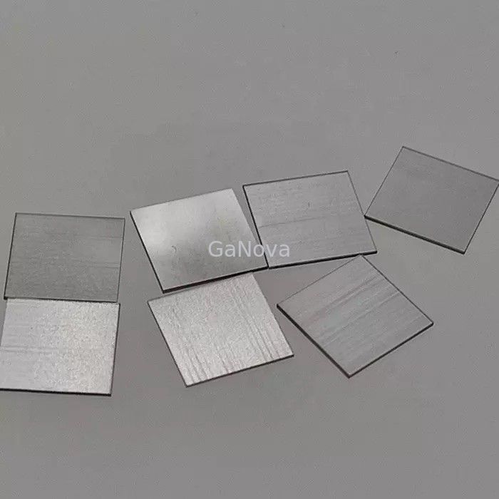
225nm to far infrared Electronic Grade Single Crystal Diamond N Content<100ppb
3*3mm²*0.3mm Electronic Grade Single Crystal Diamond,N Content<100ppb, XRD<0.015º For Heat Sink
Overview
Advantages:
1, produced by HPHT or CVD
2, high quality as natural diamond, hardness is Moh's 10, can pass diamond test pen.
3, white or yellow color, good transparency, high strengh, low impurity
4, different shape(round, square, cube), size and thickness(1.1mm to 1.7mm) are available.
Features for mono-crystal synthetic diamonds for sale
1. Regular and irregular square shape
2. High hardness and stength, great thermal stability
3. High impact resistance
4. Good diaphaneity
Specification
| properties | Synthetic diamond | |
| Density(g/cm3) | 3.515 | Intrinsic properties |
| Young’s modulus(PGa) | 1050 |
Mechanical property |
| Hardness(PGa) |
70~120single crystal 60~100 polycrystalline |
|
| Breaking strength |
2.5-3GPasingle crystal 200-1100MPa polycrystalline |
|
| Fracture toughness(MPa·m1/2) | 1~8 | |
| Firction coefficient | 0.1 | |
| Thermal conductivity(300K,Wm·K) | 1000~2000 | Thermal properties |
| Coefficient of thermal expansion(×10-6/℃) | 1(room temperature) | |
| Rerfractive index(590nm) | 2.4 | Optical properties |
| Light transmittance | 225nm to far infrared | |
| Band gap width(ev) | 5.47 | Electrical properties |
| Resistivity(Ω·cm) | >1010 | |
| Electron mobility(cm2/V·S) | 4500 | |
| Hole mobility(cm2/V·s) | 3800 | |
| Dielectric constant | 5.5 | Dielectric properties |
| Dielectric losses | <2×10⁻⁴ |
About Us
We specialize in processing a variety of materials into wafers, substrates and customized optical glass parts.components widely used in electronics, optics, opto electronics and many other fields. We also have been working closely with many domestic and oversea universities, research institutions and companies, provide customized products and services for their R&D projects. It's our vision to maintaining a good relationship of cooperation with our all customers by our good reputations.
FAQ
Q: Are you trading company or manufacturer ?
We are factory.
Q: How long is your delivery time?
Generally it is 3-5 days if the goods are in stock.
or it is 7-10 days if the goods are not in stock, it is according to quantity.
Q: Do you provide samples ? is it free or extra ?
Yes, we could offer the sample for free charge but do not pay the cost of freight.
Q: What is your terms of payment ?
Payment <=5000USD, 100% in advance.
Paymen >=5000USD, 80% T/T in advance , balance before shippment.
Contact Person: Xiwen Bai (Ciel)
Tel: +8613372109561