|
Product Details:
|
| Politype: | 4H | Diameter: | 100.0mm±0.5mm |
|---|---|---|---|
| Carrier Type: | N-type | Resistivity: | 0.015~0.028ohm.cm |
| Orientation: | 4.0°±0.2° | Primary Flat Orientation: | {10-10}±5.0° |
| Primary Flat Lengh: | 32.5mm±2.0mm | Secondary Flat Orientation: | Si-face:90°cw.from Primary Flat±5° |
| Highlight: | 4” SiC Ingot Crystal,D Grade SiC Ingot Crystal |
||
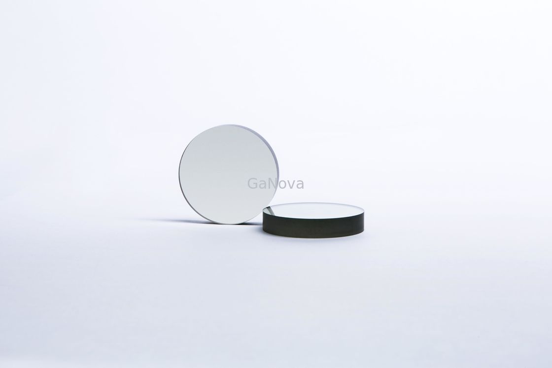
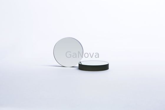
SiC ingot crystal 4" P grade
SiC devices can operate at high frequencies (RF and microwave) because of the high saturated electron drift velocity of SiC.
SiC is an excellent thermal conductor. Heat will flow more readily through SiC than other semiconductor materials. In fact, at room temperature, SiC has a higher thermal conductivity than any metal. This property enables SiC devices to operate at extremely high power levels and still dissipate the large amounts of excess heat generated.
| 6inch SiC ingot specifications | ||
| Grade | Production Grade | Dummy Grade |
| Politype | 4H | |
| Diameter | 100.0mm±0.5mm | |
| Carrier Type | N-type | |
| Resistivity | 0.015~0.028ohm.cm | |
| Orientation | 4.0°±0.2° | |
| Primary Flat Orientation | {10-10}±5.0° | |
| Primary Flat Lengh | 32.5mm±2.0mm | |
| Secondary Flat Orientation | Si-face:90°cw.from primary flat±5° | |
| Secondary Flat Length | 18.0mm±2.0mm | |
| Edge cracks by high intensity light | ≤1mm in radial | ≤3mm in radial |
| Hex Plates by high intensity light | Size<1mm,Cumulative area<1% | Cumulative area<5% |
| Polytype Areas by high intensity light | None | ≤5%area |
| MicroPipe Density | It’s destructive testing. If any disagreement, the samples for supplier retest should be provided by the customer. |
It’s destructive testing. If any disagreement, the samples for supplier retest should be provided by the customer.
|
| Edge chip | ≤1 with maximum length and width 1 mm | ≤3 with maximum length and width 3 mm |
About Us
We specialize in processing a variety of materials into wafers, substrates and customized optical glass parts.components widely used in electronics, optics, opto electronics and many other fields. We also have been working closely with many domestic and oversea universities, research institutions and companies, provide customized products and services for their R&D projects. It's our vision to maintaining a good relationship of cooperation with our all customers by our good reputations.
FAQ
Q: Are you trading company or manufacturer ?
We are factory.
Q: How long is your delivery time?
Generally it is 3-5 days if the goods are in stock.
or it is 7-10 days if the goods are not in stock, it is according to quantity.
Q: Do you provide samples ? is it free or extra ?
Yes, we could offer the sample for free charge but do not pay the cost of freight.
Q: What is your terms of payment ?
Payment <=5000USD, 100% in advance.
Paymen >=5000USD, 80% T/T in advance , balance before shippment.
Contact Person: Xiwen Bai (Ciel)
Tel: +8613372109561