|
Product Details:
|
| Politype: | 4H | Diameter: | 150.0mm±0.5mm |
|---|---|---|---|
| Carrier Type: | N-type | Resistivity: | 0.015~0.028ohm.cm |
| Orientation: | 4.0°±0.2° | Primary Flat Orientation: | {10-10}±5.0° |
| Primary Flat Lengh: | 47.5mm±2.5mm | Secondary Flat Orientation: | Si-face:90°cw.from Primary Flat±5° |
| Highlight: | P grade SiC Ingot Crystal,6” SiC Ingot Crystal |
||
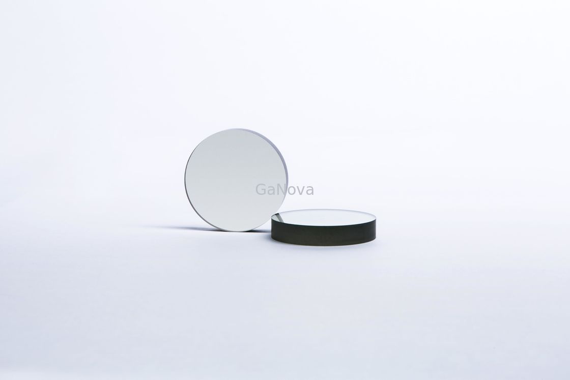
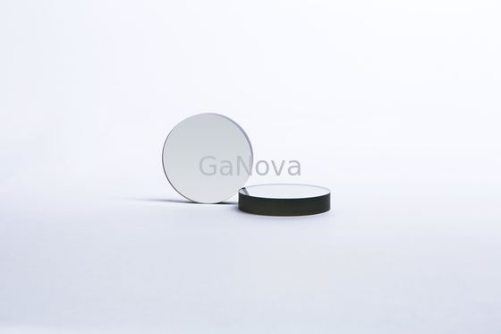
SiC ingot crystal 6" Pgrade
Silicon carbide, exceedingly hard, synthetically produced crystalline compound of silicon and carbon. Its chemical formula is SiC. Since the late 19th century silicon carbide has been an important material for sandpapers, grinding wheels, and cutting tools.
SiC can be also used as an electrical heating element because of its high electrical conductivity, good oxidation resistance, and high thermal shock resistance.
| 6inch SiC ingot specifications | ||
| Grade | Production Grade | Dummy Grade |
| Politype | 4H | |
| Diameter | 150.0mm±0.5mm | |
| Carrier Type | N-type | |
| Resistivity | 0.015~0.028ohm.cm | |
| Orientation | 4.0°±0.2° | |
| Primary Flat Orientation | {10-10}±5.0° | |
| Primary Flat Lengh | 47.5mm±2.5mm | |
| Edge cracks by high intensity light | ≤1mm in radial | ≤3mm in radial |
| Hex Plates by high intensity light | Size<1mm,Cumulative area<1% | Cumulative area<5% |
| Polytype Areas by high intensity light | None | ≤5%area |
| MicroPipe Density | It’s destructive testing. If any disagreement, the samples for supplier retest should be provided by the customer. | It’s destructive testing. If any disagreement, the samples for supplier retest should be provided by the customer. |
| Edge chip | ≤2 with maximum length and width 1 mm | ≤3 with maximum length and width 3 mm |
About Us
We specialize in processing a variety of materials into wafers, substrates and customized optical glass parts.components widely used in electronics, optics, opto electronics and many other fields. We also have been working closely with many domestic and oversea universities, research institutions and companies, provide customized products and services for their R&D projects. It's our vision to maintaining a good relationship of cooperation with our all customers by our good reputations.
FAQ
Q: Are you trading company or manufacturer ?
We are factory.
Q: How long is your delivery time?
Generally it is 3-5 days if the goods are in stock.
or it is 7-10 days if the goods are not in stock, it is according to quantity.
Q: Do you provide samples ? is it free or extra ?
Yes, we could offer the sample for free charge but do not pay the cost of freight.
Q: What is your terms of payment ?
Payment <=5000USD, 100% in advance.
Paymen >=5000USD, 80% T/T in advance , balance before shippment.
Contact Person: Xiwen Bai (Ciel)
Tel: +8613372109561