|
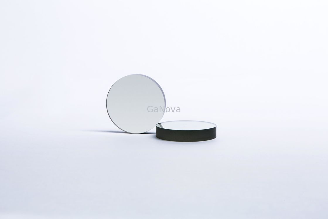
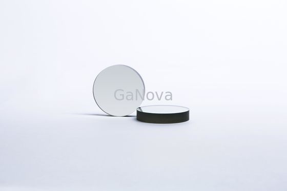
Product Details:
|
| Politype: | 4H | Diameter: | 105±0.5mm |
|---|---|---|---|
| Thickness: | 500±50μm | TTV: | ≤15μm |
| BoW(μm)/Warp(μm): | ≤45 | Crystal Orientation: | 4°off-axis Toward<11-20>±0.5° |
| Highlight: | 6inch SiC Seed Crystal |
||
JDZJ01-001-008 4&6inch SiC Seed crystal
The physical and electronic properties of SiC make it the foremost semiconductor material for short wavelength optoelectronic, high temperature, radiation resistant, and high- power/high-frequency electronic devices.
SiC can withstand a voltage gradient (or electric field) over eight times greater than than Si or GaAs without undergoing avalanche breakdown. This high breakdown electric field enables the fabrication of very high-voltage, high-power devices such as diodes, power transitors, power thyristors and surge suppressors, as well as high power microwave devices. Additionally, it allows the devices to be placed very close together, providing high device packing density for integrated circuits.
| 4&6inch SiC Seed crystal | ||
| Grade | S level | S level |
| Seed crystal specifications | 6”SiC | 6”SiC |
| Diameter(mm) | 105±0.5 | 153±0.5 |
| Thickness(μm) | 500±50 | 350±20 or 500±50 |
| TTV(μm) | ≤15 | ≤15 |
| BoW(μm)/Warp(μm) | ≤45 | ≤60 |
| Crystal orientation | 4°off-axis toward<11-20>±0.5° | 4°off-axis toward<11-20>±0.5° |
| Main positioning edge lenght | 32.5±2.0 | 18.0±2.0 |
| Subposition dege length | 18.0±2.0 | 6.0±2.0 |
| Positioning edge direction |
Si face:rotate clockwise along the main positioning side:90°±5° C face:rotate counterclockwise along the main positioning side:90°±5° |
Si face:rotate clockwise along the main positioning side:90°±5° C face:rotate counterclockwise along the main positioning side:90°±5° |
| Resistivity | 0.01~0.028Ω·cm | 0.01~0.028Ω·cm |
| Surface roughness | SSP,C face polishing,Ra≤1.0nm | DSP,C face Ra≤1.0nm |
| Single crystal zone diameter(mm) | ≥102mm | ≥150mm |
| Microtubule density | ≤1/cm2 | ≤1/cm2 |
| Collapse side | ≤1mm | ≤2mm |
| Packaging method | Single piece packing | Single piece packing |
| Remark:Single crystal zone refers to the area without crack and polytype. | ||
About Us
We specialize in processing a variety of materials into wafers, substrates and customized optical glass parts.components widely used in electronics, optics, opto electronics and many other fields. We also have been working closely with many domestic and oversea universities, research institutions and companies, provide customized products and services for their R&D projects. It's our vision to maintaining a good relationship of cooperation with our all customers by our good reputations.
FAQ
Q: Are you trading company or manufacturer ?
We are factory.
Q: How long is your delivery time?
Generally it is 3-5 days if the goods are in stock.
or it is 7-10 days if the goods are not in stock, it is according to quantity.
Q: Do you provide samples ? is it free or extra ?
Yes, we could offer the sample for free charge but do not pay the cost of freight.
Q: What is your terms of payment ?
Payment <=5000USD, 100% in advance.
Paymen >=5000USD, 80% T/T in advance , balance before shippment.
Contact Person: Xiwen Bai (Ciel)
Tel: +8613372109561