|
Product Details:
|
| Product Name: | Sic Epitaxial Wafer | Crystal Form: | 4H |
|---|---|---|---|
| Diameter: | 150.0mm+0.0/-0.2mm | Surface Orientation: | {0001}±0.2° |
| Length Of Main Reference Edge: | Notch | Length Of Secondary Reference Edge: | No Sub-reference Edges |
| Highlight: | 150mm 4H SiC Wafer,SiC Substrate 350um,4H SiC Wafer 6inch |
||
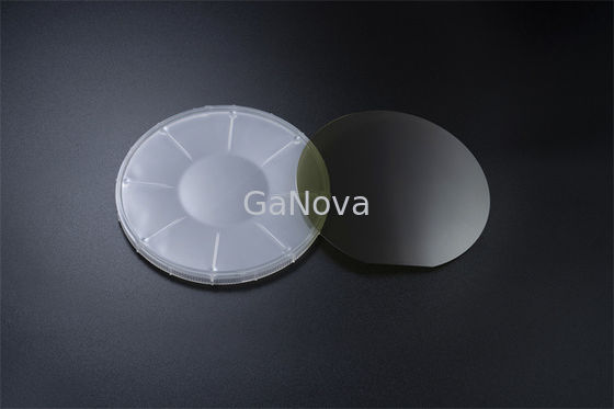
6inch 4H-SiC substrate D-level SI-Type 350.0±25.0μm MPD≤5/cm2 Resistivity≥1E5Ω·cm for power and microwave devices
Overview
Sized for improved production
With the 150 mm wafer size, we offer manufacturers the ability to leverage improved economies of scale compared with 100 mm device fabrication. Our 150 mm SiC Wafers offer consistently excellent mechanical characteristics to ensure compatibility with existing and developing device fabrication processes.
|
6inch 4H-SiC Semi insulating substrate |
|||
| Product performance | P | D | |
| Crystal form | 4H | ||
| Polytypic | Not allow | Area≤5% | |
| Micropipe Densitya | ≤0.5/cm2 | ≤5/cm2 | |
| Six square empty | Not allow | Area≤5% | |
| Hexagon surface hybrid crystal | Not allow | ||
| wrappage a | Area≤0.05% | N/A | |
| Resistivity | ≥1E9Ω·cm | ≥1E5Ω·cm | |
|
(0004)XRD Half height width of rocking curve(FWHM) |
≤45 Arcsecond |
N/A |
|
| Diameter | 150.0mm+0.0/-0.2mm | ||
| Surface orientation | {0001}±0.2° | ||
| Length of main reference edge | Notch | ||
| Length of secondary reference edge | No sub-reference edges | ||
| Notch orientation | <1-100>±1° | ||
| Notch angle | 90° +5°/-1° | ||
| Notch degree of depth | From the edge 1mm +0.25mm/-0mm | ||
| surface preparation | C-Face: Mirror Finish, Si-Face: Chemical Mechanical Polishing (CMP) | ||
| The edge of the wafer | wafer edge chamfer | ||
|
Surface roughness(10μm×10μm)
|
Si face Ra≤0.2 nm C-Face Ra≤0.5 nm
|
||
| thickness |
350.0μm±25.0μm
|
||
| LTV(10mm×10mm)a |
≤2µm
|
≤3µm
|
|
| TTVa |
≤6µm
|
≤10µm
|
|
| Bowa |
≤25µm
|
≤40µm
|
|
| Warpa |
≤40µm
|
≤60µm
|
|
| Broken edge / gap | Collapse edges of a length and a width of ≥0.5mm are not allowed | ≤2 and each length and width of ≤1.0mm | |
| scratcha | ≤5And the total length is≤ 0.5 times the diameter | ≤5 ,And the total length is≤1.5 times the diameter | |
| flaw | not allow | ||
| pollution | not allow | ||
| Edge removal |
3mm |
||
Remark: 3mm edge exclusion is used for the items marked with a.
About Us
We specialize in processing a variety of materials into wafers, substrates and customized optical glass parts.components widely used in electronics, optics, opto electronics and many other fields. We also have been working closely with many domestic and oversea universities, research institutions and companies, provide customized products and services for their R&D projects. It's our vision to maintaining a good relationship of cooperation with our all customers by our good reputations.
FAQ
Q: Are you trading company or manufacturer ?
We are factory.
Q: How long is your delivery time?
Generally it is 3-5 days if the goods are in stock.
or it is 7-10 days if the goods are not in stock, it is according to quantity.
Q: Do you provide samples ? is it free or extra ?
Yes, we could offer the sample for free charge but do not pay the cost of freight.
Q: What is your terms of payment ?
Payment <=5000USD, 100% in advance.
Paymen >=5000USD, 80% T/T in advance , balance before shippment.
Contact Person: Xiwen Bai (Ciel)
Tel: +8613372109561