|
Product Details:
|
| Dimensions: | 2 Inch | Resistivity(300K): | < 350 Ω/□ |
|---|---|---|---|
| Electron Concentration: | > 1800 Cm2/(V·S) | Substrate Structure: | 2nmGaN_cap/18-25nmAlGaN_barrier/150nmGaN_Channel/3000nmHR Buffer/500-800nmAl(Ga)N/Si(111)substrates |
| Highlight: | sic epitaxial wafer 2 Inch,Power Device sic epitaxial wafer,High Electron Mobility Transistor Epitaxial Wafer |
||
Introduction to GaN on Silicon HEMT Epi wafer
Silicon based gallium nitride HEMT epitaxial wafer is a high electron mobility transistor (HEMT) epitaxial wafer based on gallium nitride (GaN) material. Its structure mainly includes AlGaN barrier layer, GaN channel layer, AlN buffer layer, and silicon substrate. This structure enables gallium nitride HEMTs to have high electron mobility and saturation electron velocity, making them suitable for high-power and high-frequency applications.
Structural characteristics
AlGaN/GaN Heterojunction: Gallium Nitride HEMT is based on AlGaN/GaN heterojunction, which forms a high electron mobility two-dimensional electron gas (2DEG) channel through the heterojunction.
Depletion type and enhancement type: Gallium nitride HEMT epitaxial wafers are divided into depletion type (D-mode) and enhancement type (E-mode). Depleted type is the natural state of GaN power devices, while enhanced type requires special processes to achieve.
Epitaxial growth process: Epitaxial growth includes AlN nucleation layer, stress relaxation buffer layer, GaN channel layer, AlGaN barrier layer, and GaN cap layer.
manufacturing process
Epitaxial growth: Growing one or more layers of gallium nitride thin films on a silicon substrate to form high-quality epitaxial wafers.
Passivation and cap layer: SiN passivation layer and u-GaN cap layer are usually used on gallium nitride epitaxial wafers to improve surface quality and protect the epitaxial wafers.
application area
High frequency applications: Due to the high electron mobility and saturation electron velocity of gallium nitride materials, gallium nitride HEMTs are suitable for high-frequency applications such as 5G communication, radar, and satellite communication.
High power applications: Gallium nitride HEMTs perform well in high-voltage and high-power applications, suitable for fields such as electric vehicles, solar inverters, and industrial power supplies.
Product specifications
| GaN-on-Silicon HEMT Epi-wafer | ||||||
|
Item Si(111) substrates |
Al(Ga)N | HR buffer | GaN_Channel | AlGaN_barrier | GaN_cap | |
| Dimensions | 2 inch/4 inch/6inch | |||||
| Thickness | 500-800nm | 3000nm | 150nm | 18-25nm | 2nm | |
| Composition | Al% | / | / | / | 20-23 | / |
| In% | / | / | / | / | / | |
| Doping | [Si] | / | / | / | / | / |
| [Mg] | / | / | / | / | / | |
| Resistivity(300K) | < 350 Ω/□ | |||||
| Electron Concentration | > 9.0E12 cm-2 | |||||
| Mobility | > 1800 cm2/(V·S) | |||||
| Substrate Structure | 2nmGaN_cap/18-25nmAlGaN_barrier/150nmGaN_Channel/3000nmHR buffer/500-800nmAl(Ga)N/Si(111)substrates | |||||
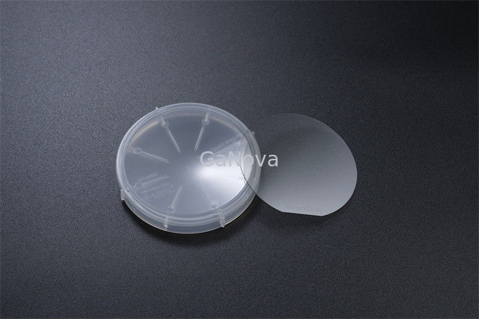
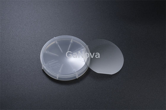
| Package | Packaged in a class 100 clean room environment, in 25PCS container, under a nitrogen atmosphere | |||||
About Us
We specialize in processing a variety of materials into wafers, substrates and customized optical glass parts.components widely used in electronics, optics, opto electronics and many other fields. We also have been working closely with many domestic and oversea universities, research institutions and companies, provide customized products and services for their R&D projects. It's our vision to maintaining a good relationship of cooperation with our all customers by our good reputations.
![]()
![]()
FAQ
Q: Are you trading company or manufacturer ?
We are factory.
Q: How long is your delivery time?
Generally it is 3-5 days if the goods are in stock.
or it is 7-10 days if the goods are not in stock, it is according to quantity.
Q: Do you provide samples ? is it free or extra ?
Yes, we could offer the sample for free charge but do not pay the cost of freight.
Q: What is your terms of payment ?
Payment <=5000USD, 100% in advance.
Paymen >=5000USD, 80% T/T in advance , balance before shippment.
Transporter
![]()
![]()
![]()
Contact Person: Xiwen Bai (Ciel)
Tel: +8613372109561