|
Product Details:
|
| Dimensions: | φ50.8mm±0.1mm,OF(1-100),Al Face,Locating Edge 16.0± 1.0mm | Substrate: | Sapphire(Single Or Double Side Polished) |
|---|---|---|---|
| Conduction Type: | Semi-Insulating | Edge Exclusion Zone: | <2mm |
| Surface Roughness: | Ra<1.5nm(10*10μm) | Product Name: | Aluminum Nitride Wafer |
| XRD FWHM Of(002): | ≤80arcsec, ≤100arcsec, ≤120arcsec, ≤160arcsec | XRD FWHM Of(102): | ≤650arcsec, ≤550arcsec, ≤450arcsec, ≤400arcsec |
| Highlight: | C-plane Sapphire Wafer,aln substrate 50.8 mm,Sapphire Wafer Side Polished |
||
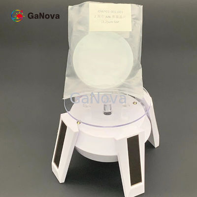
C-plane (0001)±1o AIN On Sapphire Wafer Sapphire(Single or Double Side Polished)
2 Inch Thick Film (1,2)Um AIN On Sapphire Wafer SSP XRD FWHM Of(002)≤80arcsec(102) ≤650arcsec UV Disinfection LED Chip
AlN substrate is one of the most popular ceramic substrate which has excellent heat resistance, high mechnical strength , abrasion resistance and small dielectric loss . The surface of AlN substrate is quite smooth and low porosity . Aluminium Nitride has higher thermal conductivity , compared to alumina substrate , It is about 7 to 8 times high . AlN substrate is an excellent electronic package material .
We provide AlN substrate for a wide range of applications, including thin film and thick film microelectronic , high power and high frequency circuit RF / microwave components and capacitor or resistor , contact us for more ceramic wafer product information .
| Item | AlN-T-C-U-C50 | ||
| Dimensions | φ50.8 mm±0.1 mm,OF(1-100),Al Face,Locating Edge 16.0± 1.0 mm | ||
| Substrate | Sapphire(Single or Double Side Polished) | ||
| Thickness | 1~5μm | ||
| Orientation |
C-plane (0001)±1o |
||
| Conduction Type | Semi-Insulating | ||
| Crystalline Quality | Thickness | XRD FWHM of(002) | XRD FWHM of(102) |
| [1,2)μm | ≤80arcsec | ≤650arcsec | |
| [2,3)μm | ≤100arcsec | ≤550arcsec | |
| [3,4)μm | ≤120arcsec | ≤450arcsec | |
| [4,5)μm | ≤160arcsec | ≤400arcsec | |
| Edge Exclusion Zone |
<2mm |
||
| Surface Roughness | Ra<1.5nm(10*10μm) | ||
| Package | Vacuum packing in a class 10000 clean room environment,in cassettes of 25pcs or single wafer containers. | ||
About Us
We specialize in processing a variety of materials into wafers, substrates and customized optical glass parts.components widely used in electronics, optics, opto electronics and many other fields. We also have been working closely with many domestic and oversea universities, research institutions and companies, provide customized products and services for their R&D projects. It's our vision to maintaining a good relationship of cooperation with our all customers by our good reputations.
FAQ
Q: Are you trading company or manufacturer ?
We are factory.
Q: How long is your delivery time?
Generally it is 3-5 days if the goods are in stock.
or it is 7-10 days if the goods are not in stock, it is according to quantity.
Q: Do you provide samples ? is it free or extra ?
Yes, we could offer the sample for free charge but do not pay the cost of freight.
Q: What is your terms of payment ?
Payment <=5000USD, 100% in advance.
Paymen >=5000USD, 80% T/T in advance , balance before shippment.
Contact Person: Xiwen Bai (Ciel)
Tel: +8613372109561