|
Product Details:
|
| Product Name: | AlN Single Crystal | Roughness: | Al Face:≤0.5nm N Face(back):≤1.2μm |
|---|---|---|---|
| Appearance: | Circular Belt Positioning Edge | TUA: | ≥90% |
| Main Positioning Edge Orientation: | {10-10}±5.0° | TTV(μm): | ≤30 |
| Highlight: | 1'' Aluminum Nitride Wafer,AlN Wafer S Grade,Aluminum Nitride Wafer 400um |
||
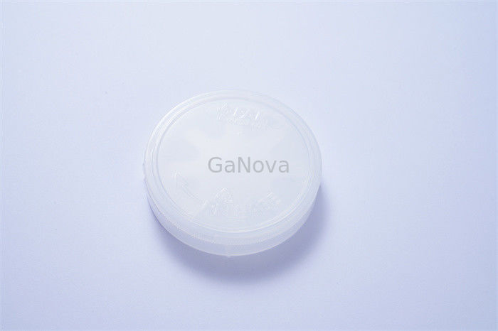
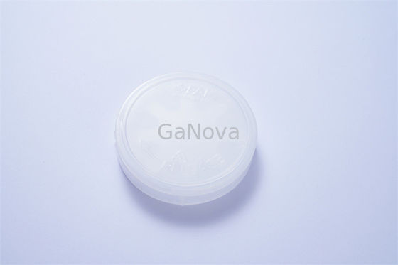
1'' AlN Single Crystal 400±50μm S/P/R Grade Aluminum Surface: Chemical Polishing Double Polishing Can Be Customized
JDCD02-001-003 1inch AlN single crystal 400±50μm S/P/R grade
What is Aluminum Nitride? Aluminum Nitride (AlN) is an excellent material to use if high thermal conductivity and electrical insulation properties are required; making it an ideal material for use in thermal management and electrical applications.
The material is stable at high temperatures under an inert atmosphere. It has a protective oxide layer that protects the material at up to 1370degC. It is also stable in hydrogen atmospheres up to 980degC. It can be dissolved or hydrolyzed by strong alkali, but is resistant to most molten salts and cryolite. This is why it is so useful in microelectronics.
| 1inch Aluminum nitride single crystal substrate | |||
| Crystal Specifications | Parameter value | ||
| Diameter(mm) | 25.4±0.5 | ||
| Thickness(μm) | 400±50 | ||
| Crystal Form | 2H | ||
| Polytype | {0001}±0.5° | ||
| Surface polishing | Aluminum surface: chemical polishing (double polishing can be customized) | ||
| Roughness |
Al face:≤0.5nm N face(back):≤1.2μm |
||
| appearance | Circular belt positioning edge | ||
| Quality grade | S grade(Super) | P grade(Prouduction) | R grade(Research) |
| HRXRD Half height width@{0002}(arcsec) | ≤150 | ≤300 | ≤500 |
| HRXRD Half height width@{10-12}(arcsec) | ≤100 | ≤200 | ≤400 |
| absorption coefficient@265nm(cm-1) | ≤50 | ≤70 | ≤100 |
| Edge Exclusion(mm) | 1 | 1 | 1 |
| Indents | / | / | / |
| Chips | / | / | ≤3 Cumulative ≤1.0mm |
| TUA | ≥90% | ||
| Main positioning edge orientation | {10-10}±5.0° | ||
| Orientation of secondary locating surface |
Al face:Rotate clockwise in the direction of the main positioning edge90°±5° N face:Rotate counterclockwise in the direction of the main positioning edge90°±5° |
||
| TTV(μm) | ≤30 | ||
| Warp(μm) | ≤30 | ||
| Bow(μm) | ≤30 | ||
| Cracks | No, naked eye, strong light | ||
| Contamination | No, naked eye, radiation | ||
| Laser coding | N face,Parallel to the main locating edge | ||
| Package | Monolithic wafer box | ||
About Us
We specialize in processing a variety of materials into wafers, substrates and customized optical glass parts.components widely used in electronics, optics, opto electronics and many other fields. We also have been working closely with many domestic and oversea universities, research institutions and companies, provide customized products and services for their R&D projects. It's our vision to maintaining a good relationship of cooperation with our all customers by our good reputations.
FAQ
Q: Are you trading company or manufacturer ?
We are factory.
Q: How long is your delivery time?
Generally it is 3-5 days if the goods are in stock.
or it is 7-10 days if the goods are not in stock, it is according to quantity.
Q: Do you provide samples ? is it free or extra ?
Yes, we could offer the sample for free charge but do not pay the cost of freight.
Q: What is your terms of payment ?
Payment <=5000USD, 100% in advance.
Paymen >=5000USD, 80% T/T in advance , balance before shippment.
Contact Person: Xiwen Bai (Ciel)
Tel: +8613372109561