|
Product Details:
|
| Dimensions: | φ50.8mm±0.1mm,OF(1-100),Al Face,Locating Edge 16.0± 1.0mm | Substrate: | Sapphire(Single Or Double Side Polished) |
|---|---|---|---|
| Conduction Type: | Semi-Insulating | Product Name: | Aluminum Nitride Wafer |
| XRD FWHM Of(002): | ≤80arcsec, ≤100arcsec, ≤120arcsec, ≤160arcsec | XRD FWHM Of(102): | ≤650arcsec, ≤550arcsec, ≤450arcsec, ≤400arcsec |
| Highlight: | AIN Sapphire Wafer,Semi Insulating AIN Wafer,Sapphire Wafer Single Side Polished |
||
2 Inch Thick Film (1,2)μm AIN On Sapphire Wafer SSP XRD FWHM Of(002)≤80arcsec(102) ≤650arcsec UV Disinfection LED Chip
The material is a good electrical insulator with excellent thermal conductivity. Its high insulating properties make it an excellent choice for a variety of applications. A wide variety of products can be made from aluminum nitride. This is the most common use for aluminum nitride. It is an important material in the aerospace industry. However, there are some limitations associated with it. It is unstable at high temperatures and in some environments.
| Item | AlN-T-C-U-C50 | ||
| Dimensions | φ50.8 mm±0.1 mm,OF(1-100),Al Face,Locating Edge 16.0± 1.0 mm | ||
| Substrate | Sapphire(Single or Double Side Polished) | ||
| Thickness | 1~5μm | ||
| Orientation |
C-plane (0001)±1o |
||
| Conduction Type | Semi-Insulating | ||
| Crystalline Quality | Thickness | XRD FWHM of(002) | XRD FWHM of(102) |
| [1,2)μm | ≤80arcsec | ≤650arcsec | |
| [2,3)μm | ≤100arcsec | ≤550arcsec | |
| [3,4)μm | ≤120arcsec | ≤450arcsec | |
| [4,5)μm | ≤160arcsec | ≤400arcsec | |
| Edge Exclusion Zone |
<2mm |
||
| Surface Roughness | Ra<1.5nm(10*10μm) | ||
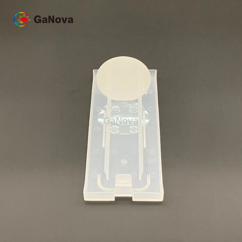
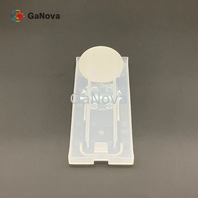
| Package | Vacuum packing in a class 10000 clean room environment,in cassettes of 25pcs or single wafer containers. | ||
About Us
We specialize in processing a variety of materials into wafers, substrates and customized optical glass parts.components widely used in electronics, optics, opto electronics and many other fields. We also have been working closely with many domestic and oversea universities, research institutions and companies, provide customized products and services for their R&D projects. It's our vision to maintaining a good relationship of cooperation with our all customers by our good reputations.
FAQ
Q: Are you trading company or manufacturer ?
We are factory.
Q: How long is your delivery time?
Generally it is 3-5 days if the goods are in stock.
or it is 7-10 days if the goods are not in stock, it is according to quantity.
Q: Do you provide samples ? is it free or extra ?
Yes, we could offer the sample for free charge but do not pay the cost of freight.
Q: What is your terms of payment ?
Payment <=5000USD, 100% in advance.
Paymen >=5000USD, 80% T/T in advance , balance before shippment.
Contact Person: Xiwen Bai (Ciel)
Tel: +8613372109561