|
Product Details:
|
| Product Name: | Aluminum Nitride Wafer | Diameter: | 25.4±0.5mm |
|---|---|---|---|
| Thickness: | 400±50μm | Crystal Form: | 2H |
| Polytype: | {0001}±0.5° | TUA: | ≥90% |
| Highlight: | 1inch Aluminum Nitride Wafer,AlN Single Crystal 400um,S Grade Aluminum Nitride Wafer |
||
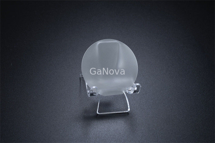
JDCD02-001-001 1inch AlN single crystal 400±50μm S/P/R grade
AlN substrate is one of the most popular ceramic substrate which has excellent heat resistance, high mechnical strength , abrasion resistance and small dielectric loss . The surface of AlN substrate is quite smooth and low porosity . Aluminium Nitride has higher thermal conductivity , compared to alumina substrate , It is about 7 to 8 times high . AlN substrate is an excellent electronic package material .
| 1inch Aluminum nitride single crystal substrate | |||
| Crystal Specifications | Parameter value | ||
| Diameter(mm) | 25.4±0.5 | ||
| Thickness(μm) | 400±50 | ||
| Crystal Form | 2H | ||
| Polytype | {0001}±0.5° | ||
| Surface polishing | Aluminum surface: chemical polishing (double polishing can be customized) | ||
| Roughness |
Al face:≤0.5nm N face(back):≤1.2μm |
||
| appearance | Circular belt positioning edge | ||
| Quality grade | S grade(Super) | P grade(Prouduction) | R grade(Research) |
| HRXRD Half height width@{0002}(arcsec) | ≤150 | ≤300 | ≤500 |
| HRXRD Half height width@{10-12}(arcsec) | ≤100 | ≤200 | ≤400 |
| absorption coefficient@265nm(cm-1) | ≤50 | ≤70 | ≤100 |
| Edge Exclusion(mm) | 1 | 1 | 1 |
| Indents | / | / | / |
| Chips | / | / | ≤3 Cumulative ≤1.0mm |
| TUA | ≥90% | ||
| Main positioning edge orientation | {10-10}±5.0° | ||
| Orientation of secondary locating surface |
Al face:Rotate clockwise in the direction of the main positioning edge90°±5° N face:Rotate counterclockwise in the direction of the main positioning edge90°±5° |
||
| TTV(μm) | ≤30 | ||
| Warp(μm) | ≤30 | ||
| Bow(μm) | ≤30 | ||
| Cracks | No, naked eye, strong light | ||
| Contamination | No, naked eye, radiation | ||
| Laser coding | N face,Parallel to the main locating edge | ||
| Package | Monolithic wafer box | ||
About Us
We specialize in processing a variety of materials into wafers, substrates and customized optical glass parts.components widely used in electronics, optics, opto electronics and many other fields. We also have been working closely with many domestic and oversea universities, research institutions and companies, provide customized products and services for their R&D projects. It's our vision to maintaining a good relationship of cooperation with our all customers by our good reputations.
FAQ
Q: Are you trading company or manufacturer ?
We are factory.
Q: How long is your delivery time?
Generally it is 3-5 days if the goods are in stock.
or it is 7-10 days if the goods are not in stock, it is according to quantity.
Q: Do you provide samples ? is it free or extra ?
Yes, we could offer the sample for free charge but do not pay the cost of freight.
Q: What is your terms of payment ?
Payment <=5000USD, 100% in advance.
Paymen >=5000USD, 80% T/T in advance , balance before shippment.
Contact Person: Xiwen Bai (Ciel)
Tel: +8613372109561