|
Product Details:
|
| Dimension: | 50.80±0.10mm | Thickness: | 430±10μm |
|---|---|---|---|
| Flat Edge Angle: | A-plane±0.2˚ | TTV: | ≤5μm |
| BOW: | ≤-8~0μm | Front Surface Roughness: | ≤0.25nm |
| Highlight: | 0.8um led sapphire substrate,Patterned Sapphire wafer,1.2um led sapphire substrate |
||
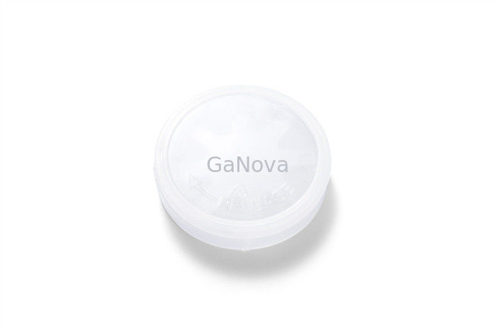
Back Surface Roughness 0.8~1.2μm Patterned Sapphire Substrates Round Edge
2inch Patterned Sapphire Substrates,LED Chip,Substrate Material
Patterned Sapphire Substrates (PSS) is a micro-patterned sapphire substrate. It has been widely used in high-power GaN-based Light Emitting Diodes (LEDs), which are the most promising alternative light source for general lighting. With the breakthrough of the patterned-sapphire substrate technique, the efficacy of high-brightness GaN-based LEDs has been driven to a record high of 150 lm/W.
| 2inch Patterned sapphire substrate | ||
| Item | Al2O3 |
|
| Dimension | 50.80±0.10mm | |
| Thickness | 430±10μm | |
| Flat edge width |
16±1.0mm |
|
| Flat edge angle | A-plane±0.2o | |
| TTV | ≤5μm | |
| BOW | ≤-8~0μm | |
| Front Surface Roughness | ≤0.25nm | |
| Back Surface Roughness | 0.8~1.2μm | |
| Edge | Round | |
| Laser making | back | |
About Us
We specialize in processing a variety of materials into wafers, substrates and customized optical glass parts.components widely used in electronics, optics, opto electronics and many other fields. We also have been working closely with many domestic and oversea universities, research institutions and companies, provide customized products and services for their R&D projects. It's our vision to maintaining a good relationship of cooperation with our all customers by our good reputations.
FAQ
Q: Are you trading company or manufacturer ?
We are factory.
Q: How long is your delivery time?
Generally it is 3-5 days if the goods are in stock.
or it is 7-10 days if the goods are not in stock, it is according to quantity.
Q: Do you provide samples ? is it free or extra ?
Yes, we could offer the sample for free charge but do not pay the cost of freight.
Q: What is your terms of payment ?
Payment <=5000USD, 100% in advance.
Paymen >=5000USD, 80% T/T in advance , balance before shippment.
Contact Person: Xiwen Bai (Ciel)
Tel: +8613372109561