|
Product Details:
|
| Features: | Blue-LED | Product Name: | Blue-LED GaN On Silicon Wafer |
|---|---|---|---|
| Dimensions: | 2 Inch | AlGaN Buffer Thickness: | 400-600nm |
| Longueur D’onde Laser: | 455±5nm | Substrate Structure: | Structure 10nmConnect Layer/pGaN/400-600nmAlGaN/70-150nmInGaN/~15nmGaN-QB/~2.5nmInGaN-QW/70-150nmInGaN/1200-1500nmAlGaN/1300-1500nmnGaN/1300-1500nmnGaN/1300-1500nmuGaN/1000nmAl(Ga)N Buffer/Si(111)substrates |
| Highlight: | 455±10nm GaN On Silicon Wafer |
||
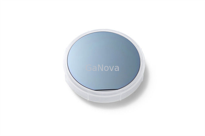
2inch Blue-LED GaN on silicon wafer
Gallium Nitride is a semiconductor technology used for high power, high-frequency semiconductor applications. Gallium Nitride exhibits several characteristics that make it better than GaAs and Silicon for various high power components. These characteristics include a higher breakdown voltage and better electrical resistivity.
| 2inch GaN blue laser on silicon | ||||||||||||
|
Item Si(111) substrates |
Al(Ga)N buffer | uGaN | nGaN | AlGaN | InGaN |
MQW (1-3 pairs) |
InGaN | AlGaN | pGaN | Contact layer | ||
| InGaN-QW | GaN-QB | |||||||||||
| Dimension | 2 inch | |||||||||||
| Thickness | 1000nm | 1300-1500nm | 1300-1500nm | 1200-1500nm | 70-150nm | ~2.5nm | ~15nm | 70-150nm | 400-600nm | / | 10nm | |
| Composition | Al% | / | / | / | 5-8 | / | / | / | / | 5-8 | / | / |
| In% | / | / | / | 2-8 | ~15 | / | 2-8 | / | / | / | ||
| Doping | [Si] | / | / | 5.0E+18 | 2.0E+18 | 2.0E+18 | / | / | / | / | / | / |
| [Mg] | / | / | / | / | / | / | / | / | 2.0E+19 | 2.0E+19 | / | |
| Longueur d’onde laser | 455±5nm | |||||||||||
| Substrate Structure | 10nmConnect layer/pGaN/400-600nmAlGaN/70-150nmInGaN/~15nmGaN-QB/~2.5nmInGaN-QW/70-150nmInGaN/1200-1500nmAlGaN/1300-1500nmnGaN/1300-1500nmnGaN/1300-1500nmuGaN/1000nmAl(Ga)N buffer/Si(111)substrates | |||||||||||
| Package | Packaged in a class 100 clean room environment, in 25PCS container, under a nitrogen atmosphere | |||||||||||
About Us
We specialize in processing a variety of materials into wafers, substrates and customized optical glass parts.components widely used in electronics, optics, opto electronics and many other fields. We also have been working closely with many domestic and oversea universities, research institutions and companies, provide customized products and services for their R&D projects. It's our vision to maintaining a good relationship of cooperation with our all customers by our good reputations.
FAQ
Q: Are you trading company or manufacturer ?
We are factory.
Q: How long is your delivery time?
Generally it is 3-5 days if the goods are in stock.
or it is 7-10 days if the goods are not in stock, it is according to quantity.
Q: Do you provide samples ? is it free or extra ?
Yes, we could offer the sample for free charge but do not pay the cost of freight.
Q: What is your terms of payment ?
Payment <=5000USD, 100% in advance.
Paymen >=5000USD, 80% T/T in advance , balance before shippment.
Contact Person: Xiwen Bai (Ciel)
Tel: +8613372109561