|
Product Details:
|
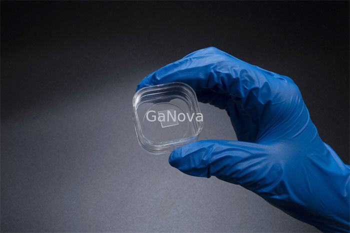
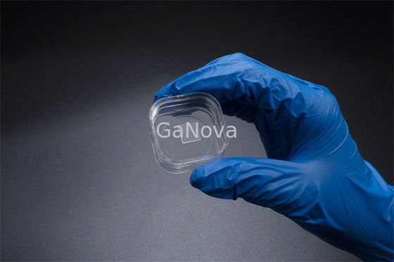
| Product Name: | Free-Standing GaN Substrates | Dimensions: | 10 X 10.5mm² |
|---|---|---|---|
| Thickness: | 350 ±25µm | TTV: | ≤ 10µm |
| BoW: | - 10µm ≤ BOW ≤ 10µm | Useable Area: | > 90% (edge Exclusion) |
| Highlight: | 350 ±25 µm GaN Substrates,10 X 10.5 mm2 GaN Substrates |
||
10*10.5mm² C-face Un-doped n-type free-standing GaN single crystal substrate Resistivity < 0.1 Ω·cm Power device/laser
Overview
GaN Substrates
GaN (gallium nitride) substrates and wafers with high quality (low dislocation density) and best prices on the market.
Premium quality free standing GaN crystal substrates with low dislocation density (on the order of 105 /cm2) and uniform surface with no periodic defects. These high-quality gallium nitride crystals have a usable area of more than 90%. Options include: N-type, P-type, Semi-insulating, C-plane, M-plane, A-plane. Sizes up to 2 inch diameter.
We sell directly from the factory, and therefore can offer the best prices on the market for high quality GaN crystal substrates.
| 10 x 10.5 mm2 Free-standing GaN Substrates | ||||
| Item | GaN-FS-C-U-S10 | GaN-FS-C-N-S10 | GaN-FS-C-SI-S10 |
Remarks: |
| Dimensions | 10 x 10.5 mm2 | |||
| Thickness | 350 ±25 µm | |||
| Orientation | C plane (0001) off angle toward M-axis 0.35 ±0.15° | |||
| Conduction Type | N-type | N-type | Semi-Insulating | |
| Resistivity(300K) | < 0.1 Ω·cm | < 0.05 Ω·cm | > 106 Ω·cm | |
| TTV | ≤ 10 µm | |||
| BoW | - 10 µm ≤ BOW ≤ 10 µm | |||
| Ga Face Surface Roughness | < 0.2 nm (polished) or < 0.3 nm (polished and surface treatment for epitaxy) |
|||
| N Face Surface Roughness | 0.5 ~1.5 μm option: 1~3 nm (fine ground); < 0.2 nm (polished) |
|||
| Dislocation Density | From 1 x 10⁵ to 3 x 106 cm-2 (calculated by CL)* | |||
| Macro Defect Density | 0 cm-2 | |||
| Useable Area | > 90% (edge exclusion) | |||
| Package | Packaged in a class 100 clean room environment, in 6 PCS container, under a nitrogen atmosphere | |||
*National standards of China (GB/T32282-2015)
![]()
About Us
We specialize in processing a variety of materials into wafers, substrates and customized optical glass parts.components widely used in electronics, optics, opto electronics and many other fields. We also have been working closely with many domestic and oversea universities, research institutions and companies, provide customized products and services for their R&D projects. It's our vision to maintaining a good relationship of cooperation with our all customers by our good reputations.
FAQ
Q: Are you trading company or manufacturer ?
We are factory.
Q: How long is your delivery time?
Generally it is 3-5 days if the goods are in stock.
or it is 7-10 days if the goods are not in stock, it is according to quantity.
Q: Do you provide samples ? is it free or extra ?
Yes, we could offer the sample for free charge but do not pay the cost of freight.
Q: What is your terms of payment ?
Payment <=5000USD, 100% in advance.
Paymen >=5000USD, 80% T/T in advance , balance before shippment.
Contact Person: Xiwen Bai (Ciel)
Tel: +8613372109561