|
Product Details:
|
| Features: | 2-4inch Blue-LED GaN On Silicon | Dimensions: | 2 Inch /4inch |
|---|---|---|---|
| AlGaN Buffer Thickness: | 600nm | Longueur D’onde Laser: | 455±10nm |
| Substrate Structure: | 20nmP++GaN/60nmP-GaN/30nmP-AlGaN/5nmGaN-QB/3nmInGaN-QW/2800nmN-GaN/800nmUndoped GaN/600nmAlGaN Buffer/330nmAIN/Si(111)substrates(1500μm) | Product Name: | GaN Epitaxial Wafer |
| Highlight: | 600nm GaN On Silicon Wafer,2inch GaN On Silicon Wafer |
||
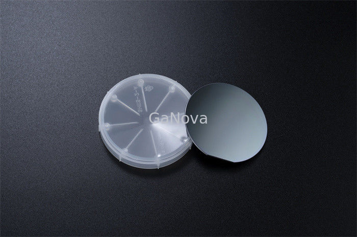
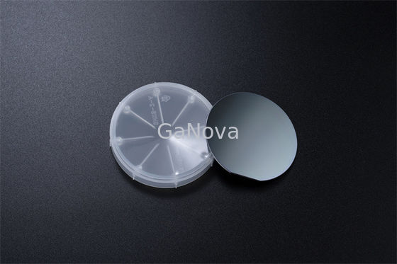
2inch Blue-LED GaN on silicon wafer
There are three main substrates that are used with GaN - Silicon Carbide (SiC), Silicon (Si) and Diamond. GaN on SiC is the most common of the three and has been used in various applications in the Military and for High Power Wireless Infrastructure Applications. GaN on Si is a newer substrate whose performance is not as good as SiC but it is more economical. GaN on Diamond is the best performing, however since it is new and relatively expensive, applications, where this has been used, are limited.
| 2-4inch Blue-LED GaN on silicon | ||||||||||
|
Item Si(111) substrates(1500μm) |
AIN | AlGaN buffer | Undoped GaN | N-GaN | MQW (7 pairs) | P-AlGaN | P-GaN |
P++GaN
|
||
| InGaN-QW | GaN-QB | |||||||||
| Dimension | 2 inch /4inch | |||||||||
| Thickness | 330nm | 600nm | 800nm | 2800nm | 3nm | 5nm | 30nm | 60nm | 20nm | |
| Composition | Al% | / | graded down | / | / | / | / | 15% | / | / |
| In% | / | / | / | / | 15% | / | / | / | / | |
| Doping | [Si] | / | / | / | 8.0E+18 | / | 2.0E+17 | / | / | / |
| [Mg] | / | / | / | / | / | / | 1.0E+20 | 3.0E+19 | 2.0E+20 | |
| Longueur d’onde laser | 455±10nm | |||||||||
| Substrate Structure | 20nmP++GaN/60nmP-GaN/30nmP-AlGaN/5nmGaN-QB/3nmInGaN-QW/2800nmN-GaN/800nmUndoped GaN/600nmAlGaN buffer/330nmAIN/Si(111)substrates(1500μm) | |||||||||
| Package | Packaged in a class 100 clean room environment, in 25PCS container, under a nitrogen atmosphere | |||||||||
About Us
We specialize in processing a variety of materials into wafers, substrates and customized optical glass parts.components widely used in electronics, optics, opto electronics and many other fields. We also have been working closely with many domestic and oversea universities, research institutions and companies, provide customized products and services for their R&D projects. It's our vision to maintaining a good relationship of cooperation with our all customers by our good reputations.
FAQ
Q: Are you trading company or manufacturer ?
We are factory.
Q: How long is your delivery time?
Generally it is 3-5 days if the goods are in stock.
or it is 7-10 days if the goods are not in stock, it is according to quantity.
Q: Do you provide samples ? is it free or extra ?
Yes, we could offer the sample for free charge but do not pay the cost of freight.
Q: What is your terms of payment ?
Payment <=5000USD, 100% in advance.
Paymen >=5000USD, 80% T/T in advance , balance before shippment.
Contact Person: Xiwen Bai (Ciel)
Tel: +8613372109561