|
Product Details:
|
| Type: | Flat Sapphire | Product Name: | 4inch GaN-on-Sapphire Blue/Green LED Wafer |
|---|---|---|---|
| Polish: | Single Side Polished (SSP) / Double Side Polished (DSP) | Dimension: | 100 ± 0.2mm |
| Orientation: | C Plane (0001) Off Angle Toward M-axis 0.2 ± 0.1° | Thickness: | 650 ± 25μm |
| Highlight: | Blue LED GaN Epitaxial Wafer,4 Inch led wafer,GaN Epitaxial Wafer C Plane |
||
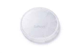
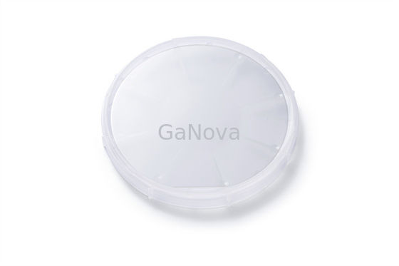
4 Inch Blue LED GaN Epitaxial Wafer On Sapphire SSP C Plane (0001) Off Angle Toward M-Axis 0.2 ± 0.1°
4 inch Blue LED GaN epitaxial wafer on sapphire SSP
Using blue radiation in LED technology offers two specific advantages – one, it consumes lesser power, two, it is more efficient in terms of light output. For instance, from 2014, to 2018, with advancement in phosphor, the efficiency of blue LEDs increased from 130-140 lm/W to 200-210 lm/W.
Another major problem in producing blue LEDs was the difficulty in p-doping GaN with precision. In the late 1980s, Amano and Akasaki discovered that when GaN was doped with zinc atoms, it emitted more light and thus this gave better p-doping. This phenomena was later explained in an article by Nakamura.
| 4inch GaN-on-Sapphire Blue/Green LED Wafer | ||||
|
Substrate |
Type | Flat Sapphire |
|
|
| Polish | Single side polished (SSP) / Double side polished (DSP) | |||
| Dimension | 100 ± 0.2 mm | |||
| Orientation | C plane (0001) off angle toward M-axis 0.2 ± 0.1° | |||
| Thickness | 650 ± 25 μm | |||
|
Epilayer |
Structure | 0.2μm pGaN/0.5μm MQWs/2.5μm nGaN/2.0μm uGaN | ||
| Thickness | 5.5 ± 0.5μm | |||
| Roughness (Ra) | <0.5 nm | |||
| Dislocation density | < 5 × 108 cm-2 | |||
| Wavelength | Blue LED | Green LED | ||
| 465 ± 10 nm | 525 ± 10 nm | |||
| Wavelength FWHMs | < 25 nm | < 40 nm | ||
| Chip Performance | Cut-in voltage@1μA | 2.3-2.5V | 2.2-2.4V | |
| Useable Area | > 90% (edge and macro defects exclusion) | |||
|
Package |
Packaged in a cleanroom in a single wafer container |
|||
About Us
We specialize in processing a variety of materials into wafers, substrates and customized optical glass parts.components widely used in electronics, optics, opto electronics and many other fields. We also have been working closely with many domestic and oversea universities, research institutions and companies, provide customized products and services for their R&D projects. It's our vision to maintaining a good relationship of cooperation with our all customers by our good reputations.
FAQ
Q: Are you trading company or manufacturer ?
We are factory.
Q: How long is your delivery time?
Generally it is 3-5 days if the goods are in stock.
or it is 7-10 days if the goods are not in stock, it is according to quantity.
Q: Do you provide samples ? is it free or extra ?
Yes, we could offer the sample for free charge but do not pay the cost of freight.
Q: What is your terms of payment ?
Payment <=5000USD, 100% in advance.
Paymen >=5000USD, 80% T/T in advance , balance before shippment.
Contact Person: Xiwen Bai (Ciel)
Tel: +8613372109561