|
Product Details:
|
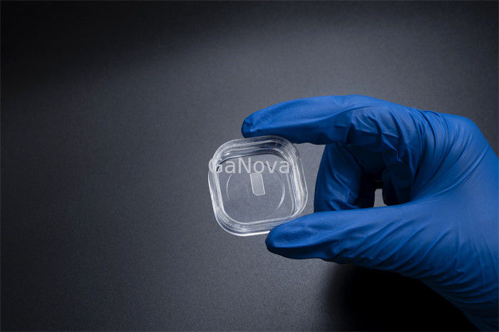
| Product Name: | GaN Substrate | Dimensions: | 5 X 10mm² |
|---|---|---|---|
| Thickness: | 350 ±25µm | TTV: | ≤ 10µm |
| BoW: | - 10µm ≤ BOW ≤ 10µm | Macro Defect Density: | 0cm⁻² |
| Highlight: | 5 X 10.5 mm2 GaN Epitaxial Wafer,325um gan gallium nitride wafer,GaN Epitaxial Wafer 375um |
||
5 X 10 mm2 M Face Free-Standing GaN Substrates Thickness 350 ±25 µm
5*10mm2 M-face Un-doped n-type free-standing GaN single crystal substrate Resistivity < 0.05 Ω·cm Power device/laser wafer
Overview
These GaN wafers realize unprecedented ultra-bright laser diodes and high-efficiency power devices for use in projector light sources, inverters for electric vehicles, and other applications.
The features are high crystalline, good uniformity, and superior surface quality. GaN substrates are used for LD applications (violet, blue and green).
| M face Free-standing GaN Substrates | ||||
| Item |
GaN-FS-M-U-S
|
GaN-FS-M-N-S
|
GaN-FS-M-SI-S |
Remarks: A circular arc angle (R < 2 mm) is used for distinguishing the front and back surface. |
| Dimensions | 5 x 10 mm2 | |||
| Thickness | 350 ±25 µm | |||
| Orientation |
M plane (1- 100) off angle toward A-axis 0 ±0.5° M plane (1- 100) off angle toward C-axis - 1 ±0.2° |
|||
| Conduction Type | N-type | N-type | Semi-Insulating | |
| Resistivity (300K) | < 0.1 Ω·cm | < 0.05 Ω·cm | > 106 Ω·cm | |
| TTV | ≤ 10 µm | |||
| BOW | - 10 µm ≤ BOW ≤ 10 µm | |||
| Front Surface Roughness |
< 0.2 nm (polished); or < 0.3 nm (polished and surface treatment for epitaxy) |
|||
| Back Surface Roughness |
0.5 ~1.5 μm option: 1~3 nm (fine ground); < 0.2 nm (polished) |
|||
| Dislocation Density | From 1 x 10⁵ to 3 x 106 cm-2 | |||
| Macro Defect Density | 0 cm-2 | |||
| Useable Area | > 90% (edge exclusion) | |||
| Package | Packaged in a class 100 clean room environment, in 6 PCS container, under a nitrogen atmosphere | |||
Appendix: The diagram of miscut angle
![]()
If δ1= 0 ±0.5 degree, then M plane (1- 100) off angle toward A-Axis is 0 ±0.5 degree.
If δ2= - 1 ±0.2 degree, then M plane (1- 100) off angle toward C-Axis is - 1 ±0.2 degree.
About Us
We specialize in processing a variety of materials into wafers, substrates and customized optical glass parts.components widely used in electronics, optics, opto electronics and many other fields. We also have been working closely with many domestic and oversea universities, research institutions and companies, provide customized products and services for their R&D projects. It's our vision to maintaining a good relationship of cooperation with our all customers by our good reputations.
FAQ
Q: Are you trading company or manufacturer ?
We are factory.
Q: How long is your delivery time?
Generally it is 3-5 days if the goods are in stock.
or it is 7-10 days if the goods are not in stock, it is according to quantity.
Q: Do you provide samples ? is it free or extra ?
Yes, we could offer the sample for free charge but do not pay the cost of freight.
Q: What is your terms of payment ?
Payment <=5000USD, 100% in advance.
Paymen >=5000USD, 80% T/T in advance , balance before shippment.
Contact Person: Xiwen Bai (Ciel)
Tel: +8613372109561