|
Product Details:
|
| Highlight: | GaN Gallium Nitride Single Crystal Substrate,2inch Gallium Nitride Single Crystal Substrate |
||
|---|---|---|---|
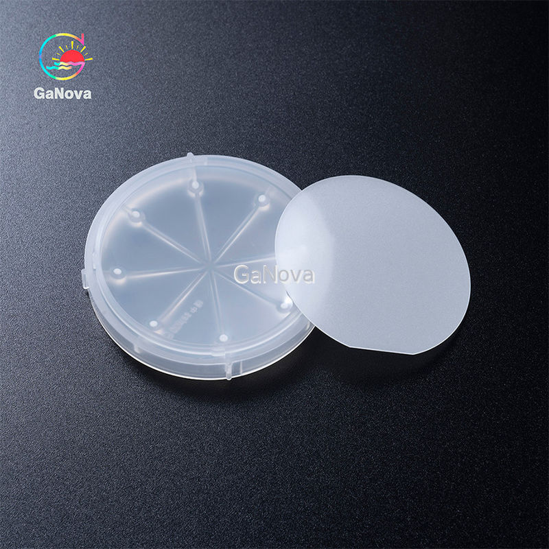
Un-Doped Freestanding GaN Substrate
1, Overview of Gallium Nitride Single Crystal Substrate(GaN substrate)
Gallium nitride single crystal substrate (GaN substrate)is an important component required in the preparation process of gallium nitride (GaN) crystals, and it is the substrate on which gallium nitride crystals are grown. Gallium nitride (GaN)crystals have a wide range of application scenarios, including LEDs, high-speed electronic devices, and power electronic devices. The quality of gallium nitride single crystal substrate(GaN substrate) has a crucial impact on the performance and yield of the crystal.
2,Product specifications
| 2-inch Free-standing U-GaN/SI-GaN Substrates | |||||||
|
Excellent level (S) |
Production level(A) |
Research level (B) |
Dummy level (C) |
Note: (1) Useable area: edge and macro defects exclusion (2) 3 points: the miscut angles of positions (2, 4, 5) are 0.35 ± 0.15o |
|||
| S-1 | S-2 | A-1 | A-2 | ||||
| Dimensions | 50.8 ± 1 mm | ||||||
| Thickness | 350 ± 25 μm | ||||||
| Orientation flat | (1-100) ± 0.5o, 16 ± 1 mm | ||||||
| Secondary orientation flat | (11-20) ± 3o, 8 ± 1 mm | ||||||
| Resistivity (300K) |
< 0.5 Ω·cm for N-type (Undoped; GaN-FS-C-U-C50) or > 1 x 10⁶ Ω·cm for Semi-insulating (Fe-doped; GaN-FS-C-SI-C50) |
||||||
| TTV | |||||||
| BOW | ≤ 20 μm ≤ 40 μm | ||||||
| Ga face surface roughness |
< 0.2 nm (polished) or < 0.3 nm (polished and surface treatment for epitaxy) |
||||||
| N face surface roughness |
0.5 ~1.5 μm option: 1~3 nm (fine ground); < 0.2 nm (polished) |
||||||
| Package | Packaged in a cleanroom in single wafer container | ||||||
| Useable area | > 90% | >80% | >70% | ||||
| Dislocation density | <9.9x105 cm-2 | <3x106 cm-2 | <9.9x105 cm-2 | <3x106 cm-2 | <3x106 cm-2 | ||
| Orientation:C plane (0001) off angle toward M-axis |
0.35 ± 0.15o (3 points) |
0.35 ± 0.15o (3 points) |
0.35 ± 0.15o (3 points) |
||||
| Macro defect density (hole) | 0 cm-2 | < 0.3 cm-2 | < 1 cm-2 | ||||
| Max size of macro defects | < 700 μm | < 2000 μm | < 4000 μm | ||||
About Us
We specialize in processing a variety of materials into wafers, substrates and customized optical glass parts.components widely used in electronics, optics, opto electronics and many other fields. We also have been working closely with many domestic and oversea universities, research institutions and companies, provide customized products and services for their R&D projects. It's our vision to maintaining a good relationship of cooperation with our all customers by our good reputations.
![]()
![]()
FAQ
Q: Are you trading company or manufacturer ?
We are factory.
Q: How long is your delivery time?
Generally it is 3-5 days if the goods are in stock.
or it is 7-10 days if the goods are not in stock, it is according to quantity.
Q: Do you provide samples ? is it free or extra ?
Yes, we could offer the sample for free charge but do not pay the cost of freight.
Q: What is your terms of payment ?
Payment <=5000USD, 100% in advance.
Paymen >=5000USD, 80% T/T in advance , balance before shippment.
Transporter
![]()
![]()
![]()
Contact Person: Xiwen Bai (Ciel)
Tel: +8613372109561