|
Product Details:
|
| Highlight: | 4 Inch gan substrate,Fe Doped gan substrate,Freestanding gan substrate |
||
|---|---|---|---|
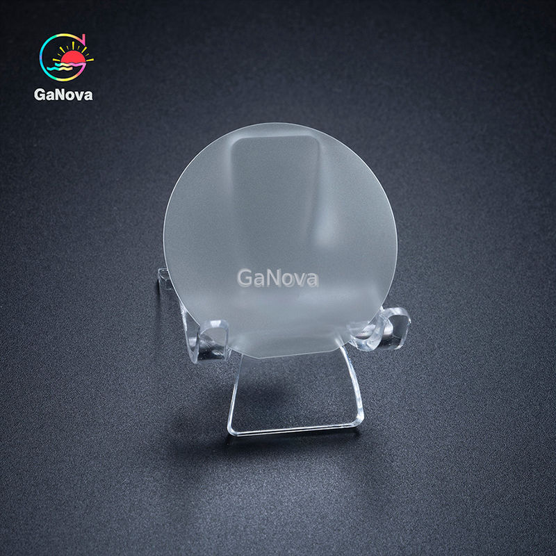
Introduction to 4-inch iron doped gallium nitride (GaN) single crystal substrate
4-inch iron doped gallium nitride (GaN) single crystal substrate is a single crystal substrate made of gallium nitride (GaN) material, which improves its electrical properties by doping iron elements. Gallium nitride (GaN) is a wide bandgap semiconductor material with a direct bandgap of 3.4 eV, which makes it widely used in optoelectronic and power electronic devices.
Preparation process
The process for preparing a 4-inch iron doped gallium nitride single crystal substrate includes:
MOCVD technology: used for growing high-quality gallium nitride single crystal layer 4.
Laser exfoliation technology: used to remove defects in single crystal layers and improve substrate performance.
HVPE technology: used for large-scale production of gallium nitride substrates to improve production efficiency.
In summary, 4-inch iron doped gallium nitride single crystal substrate is a high-performance semiconductor material with broad application prospects, especially in the fields of optoelectronics and power electronics.
Product specifications
| 2-inch Free-standing N-GaN Substrates | ||||||
|
Production level(P) |
Research(R) |
Dummy(D) |
Note: (1) 5 points: the miscut angles of 5 positions are 0.55 ±0.15o (2) 3 points: the miscut angles of positions (2, 4, 5) are 0.55 ±0.15o (3) Useable area: exclusion of periphery and macro defects (holes) |
|||
| P+ | P | P- | ||||
| Item | GaN-FS-C-N-C50-SSP | |||||
| Dimensions | 50.0 ±0.3 mm | |||||
| Thickness | 400 ± 30 μm | |||||
| Orientation flat | (1- 100) ±0.1o, 12.5 ± 1 mm | |||||
| TTV | ≤ 15 μm | |||||
| BOW | ≤ 20 μm | |||||
| Resistivity (300K) | ≤ 0.02 Ω·cm for N-type (Si-doped) | |||||
| Ga face surface roughness | ≤ 0.3 nm (polished and surface treatment for epitaxy) | |||||
| N face surface roughness | 0.5 ~1.5 μm (single side polished) | |||||
| C plane (0001) off angle toward M-axis(miscut angles) |
0.55 ± 0.1o (5 points) |
0.55± 0.15o (5 points) |
0.55 ± 0.15o (3 points) |
|||
| Threading dislocation density | ≤ 7.5 x 105 cm-2 | ≤ 3 x 106 cm-2 | ||||
| Number and max size of holes in Ф47 mm in the center | 0 | ≤ 3@1000 μm | ≤ 12@1500 μm | ≤ 20@3000 μm | ||
| Useable area | > 90% | >80% | >70% | |||
| Package | Packaged in a cleanroom in single wafer container | |||||
About Us
We specialize in processing a variety of materials into wafers, substrates and customized optical glass parts.components widely used in electronics, optics, opto electronics and many other fields. We also have been working closely with many domestic and oversea universities, research institutions and companies, provide customized products and services for their R&D projects. It's our vision to maintaining a good relationship of cooperation with our all customers by our good reputations.
![]()
![]()
FAQ
Q: Are you trading company or manufacturer ?
We are factory.
Q: How long is your delivery time?
Generally it is 3-5 days if the goods are in stock.
or it is 7-10 days if the goods are not in stock, it is according to quantity.
Q: Do you provide samples ? is it free or extra ?
Yes, we could offer the sample for free charge but do not pay the cost of freight.
Q: What is your terms of payment ?
Payment <=5000USD, 100% in advance.
Paymen >=5000USD, 80% T/T in advance , balance before shippment.
Transporter
![]()
![]()
![]()
Contact Person: Xiwen Bai (Ciel)
Tel: +8613372109561