|
Product Details:
|
| Product Name: | Single Crystal Substrate | Orientation: | (201) |
|---|---|---|---|
| Polished Surface: | Single Side Polished | FWHM: | <350arcsec |
| Ra: | ≤0.3nm | Thickness: | 0.6~0.8mm |
| Highlight: | Ga2O3 Single Crystal Substrate,Gallium Oxide wafer 0.6mm,0.8mm Single Crystal Substrate |
||
10x10mm2 (-201) Fe-doped free-standing Ga2O3 single crystal substrate Product grade single polishing Thickness 0.6~0.8mm FWHM<350arcsec,Ra≤0.3 nm Optoelectronic devices, insulating layers of semiconductor materials, and UV filters
Gallium Nitride (GaN) substrate is a high-quality single-crystal substrate. It is made with original HVPE method and wafer processing technology, which has been originally developed for many years. The features are high crystalline, good uniformity, and superior surface quality.
The purpose of this review is to summarize recent advances in the growth, processing and device performance of the most widely studied polymorph, β-Ga2O3. The role of defects and impurities on the transport and optical properties of bulk, epitaxial and nanostructures material, the difficulty in p-type doping and the development of processing techniques like etching, contact formation, dielectrics for gate formation and passivation are discussed.
| Gallium nitride substrate--Product level | ||
| Dimensions | 10*15mm | 10*10mm |
| Thickness | 0.6~0.8mm | |
| Orientation | (201) | |
| Doping | Fe | Sn |
| Polished surface | Single side polished | |
| Resistivity/Nd-Na | / | <9E18 |
| FWHM | <350arcsec | |
| Ra | ≤0.3nm | |
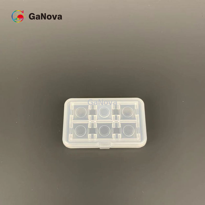
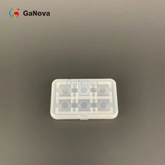
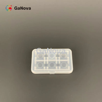
| Package | Packaged in a class 100 clean room environment, under a nitrogen atmosphere | |
About Us
We specialize in processing a variety of materials into wafers, substrates and customized optical glass parts.components widely used in electronics, optics, opto electronics and many other fields. We also have been working closely with many domestic and oversea universities, research institutions and companies, provide customized products and services for their R&D projects. It's our vision to maintaining a good relationship of cooperation with our all customers by our good reputations.
FAQ
Q: Are you trading company or manufacturer ?
We are factory.
Q: How long is your delivery time?
Generally it is 3-5 days if the goods are in stock.
or it is 7-10 days if the goods are not in stock, it is according to quantity.
Q: Do you provide samples ? is it free or extra ?
Yes, we could offer the sample for free charge but do not pay the cost of freight.
Q: What is your terms of payment ?
Payment <=5000USD, 100% in advance.
Paymen >=5000USD, 80% T/T in advance , balance before shippment.
Contact Person: Xiwen Bai (Ciel)
Tel: +8613372109561