|
Product Details:
|
| Ra: | ≤0.5nm | Thickness: | 0.6~0.8mm |
|---|---|---|---|
| Product Name: | Single Crystal Substrate | Polished Surface: | Single Side Polished |
| Orientation: | (010) | FWHM: | <350arcsec |
| Highlight: | side polished Ga2O3 Substrate,0.8mm Gallium Oxide substrate,Ga2O3 Substrate Single Crystal |
||
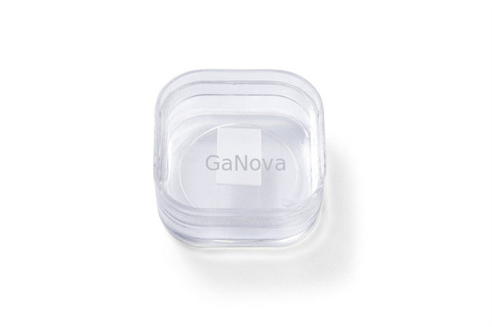
Single side polished Ga2O3 Single Crystal Substrate Thickness 0.6~0.8mm
10x15mm2(010)Sn-doped free-standing Ga2O3 single crystal substrate Product grade single polishing Thickness 0.6~0.8mm FWHM<350arcsec,Ra≤0.5nm Resistance 2.00E+17Ω/cm-3 Optoelectronic devices, insulating layers of semiconductor materials, and UV filters
GaN is growing in importance because of its ability to offer significantly improved performance across a wide range of applications while reducing the energy and the physical space needed to deliver that performance when compared with conventional silicon technologies.
Silicon has long been the material of choice for the manufacturing of key electronics, including everything from computers and smartphones to televisions and cameras.
| Gallium nitride substrate--Research level | ||
| Dimension | 10*15mm | 10*10mm |
| Thickness | 0.6~0.8mm | |
| Orientation | (010) | |
| Doping | Sn | |
| Polished surface | Single side polished | |
| Resistivity/Nd-Na | 2.00E+17 | 1.53E+18 |
| FWHM | <350arcsec | |
| Ra | ≤0.5nm | |
| Package | Packaged in a class 100 clean room environment, under a nitrogen atmosphere | |
About Us
We specialize in processing a variety of materials into wafers, substrates and customized optical glass parts.components widely used in electronics, optics, opto electronics and many other fields. We also have been working closely with many domestic and oversea universities, research institutions and companies, provide customized products and services for their R&D projects. It's our vision to maintaining a good relationship of cooperation with our all customers by our good reputations.
FAQ
Q: Are you trading company or manufacturer ?
We are factory.
Q: How long is your delivery time?
Generally it is 3-5 days if the goods are in stock.
or it is 7-10 days if the goods are not in stock, it is according to quantity.
Q: Do you provide samples ? is it free or extra ?
Yes, we could offer the sample for free charge but do not pay the cost of freight.
Q: What is your terms of payment ?
Payment <=5000USD, 100% in advance.
Paymen >=5000USD, 80% T/T in advance , balance before shippment.
Contact Person: Xiwen Bai (Ciel)
Tel: +8613372109561