|
Product Details:
|
| Product Name: | GaAs-Si Wafer | Growth Method: | VGF |
|---|---|---|---|
| Conduct Type: | S-C-N | Orientation Angle: | 0° |
| IF Orientation: | EJ[0-11]±0.5° | IF Length(mm): | 7±1 |
| Diameter(mm): | 50.8±0.2 | CC(/c.c.): | 0.4E18~1E18 |
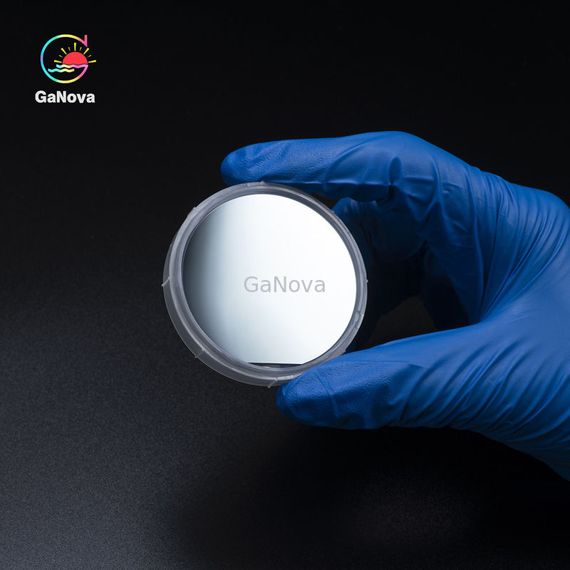
2inch GaAs (100) Si-doped substrates
Overview
GaAs is often used as a substrate material for the epitaxial growth of other III-V semiconductors, including indium gallium arsenide, aluminum gallium arsenide and others.
Gallium arsenide of a GaAs Wafer has the attribute of generating laser light from electricity in a direct manner. There are two types of GaAs Wafer; polycrystalline and single crystal. These wafers are utilized in micro electronics and opto electronics production in order to make LED, microwave circuits and LD.
|
GaAs-Si Wafer |
|
|
Growth Method |
VGF |
| Conduct Type | S-C-N |
| Dopant | GaAs-Si |
| Orientation | (100)15°±0.5° Off Toward<111>A |
| Orientation Angle | 0° |
| OF Orientation | EJ[0-1-1]±0.5° |
| OF Length (mm) | 17±1 |
| IF Orientation | EJ[0-11]±0.5° |
| IF Length(mm) | 7±1 |
| Diameter(mm) | 50.8±0.2 |
| CC(/c.c.) | 0.4E18~1E18 |
| Resistivity(ohm.cm) | N/A |
| Mobility(cm2/v.s) | ≥1000 |
| EPD(/cm2) | ≤5000 |
| Thickness(um) | 350±20 |
| TTV(um) | <10 |
| TTR(um) | <10 |
| Bow(um) | <15 |
| Warp(um) | <15 |
| Surface | Side1:Polished Side2:Etched |
| Packaging | Cassette or single |
About Us
We specialize in processing a variety of materials into wafers, substrates and customized optical glass parts.components widely used in electronics, optics, opto electronics and many other fields. We also have been working closely with many domestic and oversea universities, research institutions and companies, provide customized products and services for their R&D projects. It's our vision to maintaining a good relationship of cooperation with our all customers by our good reputations.
FAQ
Q: Are you trading company or manufacturer ?
We are factory.
Q: How long is your delivery time?
Generally it is 3-5 days if the goods are in stock.
or it is 7-10 days if the goods are not in stock, it is according to quantity.
Q: Do you provide samples ? is it free or extra ?
Yes, we could offer the sample for free charge but do not pay the cost of freight.
Q: What is your terms of payment ?
Payment <=5000USD, 100% in advance.
Paymen >=5000USD, 80% T/T in advance , balance before shippment.
Contact Person: Xiwen Bai (Ciel)
Tel: +8613372109561