|
Product Details:
|
| Growth Method: | VGF | Conduct Type: | S-C-N |
|---|---|---|---|
| Product Name: | GaAs (100) Undoped Substrates | Dopant: | GaAs-Si |
| Orientation Angle: | 0° | OF Orientation: | EJ[0-1-1]±0.5° |
| Highlight: | GaAs Epi Wafer Undoped Substrates,GaAs-Si Wafer 2inch,2inch GaAs Epi Wafer |
||
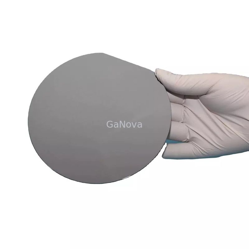
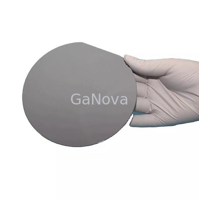
GaAs-Si Wafer 2inch GaAs (100) Undoped Substrates EJ[0-1-1]±0.5°
Overview
GaAs applications cover a large variety of transistors for industry spanning optical fiber communication, wireless networks (WLAN), mobile handsets, blue tooth communications, satellite communications, monolithic microwave integrated circuits (MMIC) for 5G, as well as radio frequency integrated circuits (RFIC).
|
GaAs-Si Wafer |
|
|
Growth Method |
VGF |
| Conduct Type | S-C-N |
| Dopant | GaAs-Si |
| Orientation | (100)15°±0.5° Off Toward<111>A |
| Orientation Angle | 0° |
| OF Orientation | EJ[0-1-1]±0.5° |
| OF Length (mm) | 17±1 |
| IF Orientation | EJ[0-11]±0.5° |
| IF Length(mm) | 7±1 |
| Diameter(mm) | 50.8±0.2 |
| CC(/c.c.) | 0.4E18~1E18 |
| Resistivity(ohm.cm) | N/A |
| Mobility(cm2/v.s) | ≥1000 |
| EPD(/cm2) | ≤5000 |
| Thickness(um) | 350±20 |
| TTV(um) | <10 |
| TTR(um) | <10 |
| Bow(um) | <15 |
| Warp(um) | <15 |
| Surface | Side1:Polished Side2:Etched |
| Packaging | Cassette or single |
About Us
We specialize in processing a variety of materials into wafers, substrates and customized optical glass parts.components widely used in electronics, optics, opto electronics and many other fields. We also have been working closely with many domestic and oversea universities, research institutions and companies, provide customized products and services for their R&D projects. It's our vision to maintaining a good relationship of cooperation with our all customers by our good reputations.
FAQ
Q: Are you trading company or manufacturer ?
We are factory.
Q: How long is your delivery time?
Generally it is 3-5 days if the goods are in stock.
or it is 7-10 days if the goods are not in stock, it is according to quantity.
Q: Do you provide samples ? is it free or extra ?
Yes, we could offer the sample for free charge but do not pay the cost of freight.
Q: What is your terms of payment ?
Payment <=5000USD, 100% in advance.
Paymen >=5000USD, 80% T/T in advance , balance before shippment.
Contact Person: Xiwen Bai (Ciel)
Tel: +8613372109561