|
Product Details:
|
| Product Name: | GaAs-Si Wafer | Orientation Angle: | 0° |
|---|---|---|---|
| OF Orientation: | EJ[0-1-1]±0.5° | OF Length (mm): | 17±1 |
| IF Orientation: | EJ[0-11]±0.5° | IF Length(mm): | 7±1 |
| Diameter(mm): | 50.8±0.2 | CC(/c.c.): | 0.4E18~1E18 |
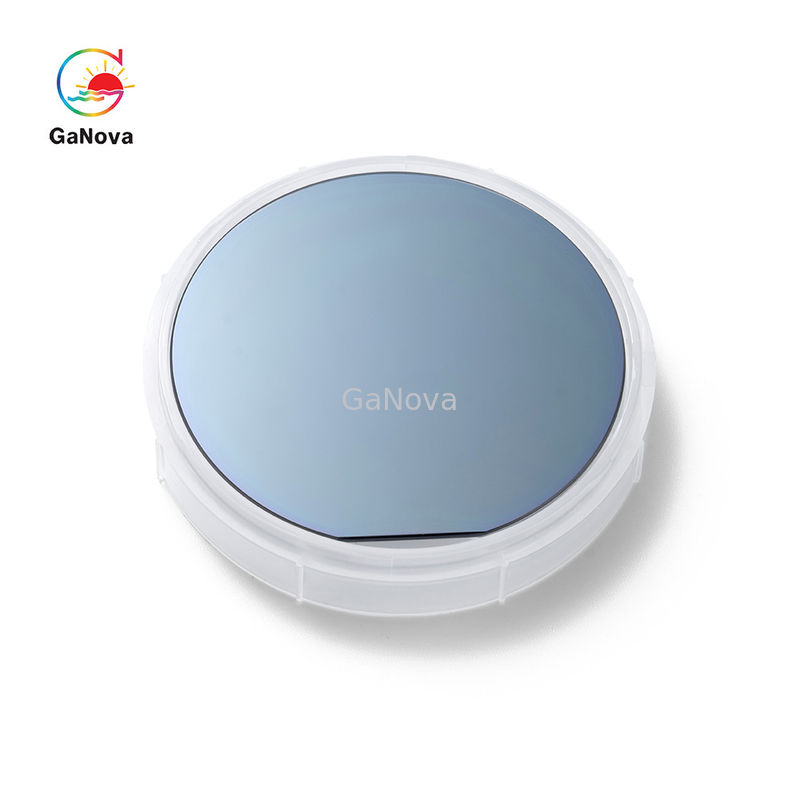
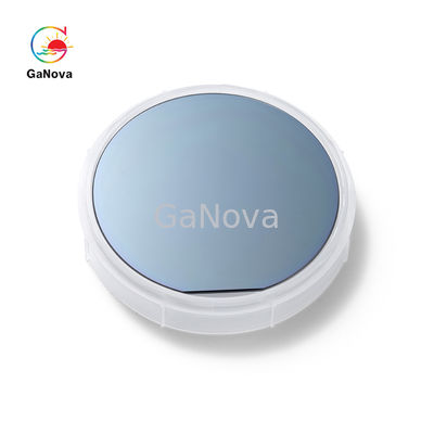
2inch GaAs (111) Si-doped substrates
Overview
Gallium in a GaAs Wafer is in general used in the production of semiconductors, barometers, light emitting diodes, thermometers and electronic circuits. It is a silvery metal and quite soft which makes it easy to be used in chips as well. Gallium element, which is a kind of post transitional metal, has the ability to bond easily with most of the metals on earth. It is highly deployed in the production of low melting alloys.
|
GaAs-Si Wafer |
|
|
Growth Method |
VGF |
| Conduct Type | S-C-N |
| Dopant | GaAs-Si |
| Orientation | (100)15°±0.5° Off Toward<111>A |
| Orientation Angle | 0° |
| OF Orientation | EJ[0-1-1]±0.5° |
| OF Length (mm) | 17±1 |
| IF Orientation | EJ[0-11]±0.5° |
| IF Length(mm) | 7±1 |
| Diameter(mm) | 50.8±0.2 |
| CC(/c.c.) | 0.4E18~1E18 |
| Resistivity(ohm.cm) | N/A |
| Mobility(cm2/v.s) | ≥1000 |
| EPD(/cm2) | ≤5000 |
| Thickness(um) | 350±20 |
| TTV(um) | <10 |
| TTR(um) | <10 |
| Bow(um) | <15 |
| Warp(um) | <15 |
| Surface | Side1:Polished Side2:Etched |
| Packaging | Cassette or single |
About Us
We specialize in processing a variety of materials into wafers, substrates and customized optical glass parts.components widely used in electronics, optics, opto electronics and many other fields. We also have been working closely with many domestic and oversea universities, research institutions and companies, provide customized products and services for their R&D projects. It's our vision to maintaining a good relationship of cooperation with our all customers by our good reputations.
FAQ
Q: Are you trading company or manufacturer ?
We are factory.
Q: How long is your delivery time?
Generally it is 3-5 days if the goods are in stock.
or it is 7-10 days if the goods are not in stock, it is according to quantity.
Q: Do you provide samples ? is it free or extra ?
Yes, we could offer the sample for free charge but do not pay the cost of freight.
Q: What is your terms of payment ?
Payment <=5000USD, 100% in advance.
Paymen >=5000USD, 80% T/T in advance , balance before shippment.
Contact Person: Xiwen Bai (Ciel)
Tel: +8613372109561