|
Product Details:
|
| Growth Method: | VGF | Conduct Type: | S-C-N |
|---|---|---|---|
| Product Name: | GaAs-Si Wafer | OF Orientation: | EJ[0-1-1]±0.5° |
| OF Length (mm): | 17±1 | IF Orientation: | EJ[0-11]±0.5° |
| Highlight: | 2inch gaas wafer,gallium arsenide substrate 7mm,51mm gaas wafer |
||
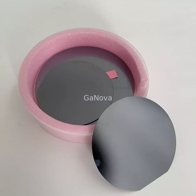
50.8±0.2mm 2inch GaAs (100) Undoped Substrates 7±1mm IF Length
Overview
With the development of mini-LED and micro-LED, red light LEDs produced with GaAs substrates are increasingly used for display screens and in AR/VR.
The conversion efficiency of a high-efficiency solar-cell panel based on GaAs is up to 40%. At present, such solar-cell panels are widely used in unmanned aerial vehicle and solar auto applications.
|
GaAs-Si Wafer |
|
|
Growth Method |
VGF |
| Conduct Type | S-C-N |
| Dopant | GaAs-Si |
| Orientation | (100)15°±0.5° Off Toward<111>A |
| Orientation Angle | 0° |
| OF Orientation | EJ[0-1-1]±0.5° |
| OF Length (mm) | 17±1 |
| IF Orientation | EJ[0-11]±0.5° |
| IF Length(mm) | 7±1 |
| Diameter(mm) | 50.8±0.2 |
| CC(/c.c.) | 0.4E18~1E18 |
| Resistivity(ohm.cm) | N/A |
| Mobility(cm2/v.s) | ≥1000 |
| EPD(/cm2) | ≤5000 |
| Thickness(um) | 350±20 |
| TTV(um) | <10 |
| TTR(um) | <10 |
| Bow(um) | <15 |
| Warp(um) | <15 |
| Surface | Side1:Polished Side2:Etched |
| Packaging | Cassette or single |
About Us
We specialize in processing a variety of materials into wafers, substrates and customized optical glass parts.components widely used in electronics, optics, opto electronics and many other fields. We also have been working closely with many domestic and oversea universities, research institutions and companies, provide customized products and services for their R&D projects. It's our vision to maintaining a good relationship of cooperation with our all customers by our good reputations.
FAQ
Q: Are you trading company or manufacturer ?
We are factory.
Q: How long is your delivery time?
Generally it is 3-5 days if the goods are in stock.
or it is 7-10 days if the goods are not in stock, it is according to quantity.
Q: Do you provide samples ? is it free or extra ?
Yes, we could offer the sample for free charge but do not pay the cost of freight.
Q: What is your terms of payment ?
Payment <=5000USD, 100% in advance.
Paymen >=5000USD, 80% T/T in advance , balance before shippment.
Contact Person: Xiwen Bai (Ciel)
Tel: +8613372109561